Characterization of Electrodeposited Cobalt/Copper (Co/Cu) Granular Multilayered Thin Films onto the Anodic Aluminum Oxide (AAO) Substrates
Herein, we report on the characterization of a series of cobalt/copper granular thin films alloys electrodeposited onto the previously pre-treated aluminum substrates, at different deposition time. And a systematic study of their structural and magneto-optical properties were investigated. The proper deposition potentials of Co, and Cu were obtained from the cyclic voltammetry method. It was observed that the easy axis direction of magnetization was parallel to the film plane for all films. The X-ray diffraction (XRD) results revealed that all films had a mixture of hexagonal close-packed (hcp) and face centered cubic (fcc) phases. The Scanning electron microscope images (SEM) and atomic force microscopy (AFM) showed some parallelepiped and ellipsoid shaped rods with an averaged dimension about of 600 nm length, 600 nm width and 200 nm thickness for a sample electrodeposited at room temperature. These rods are irregularly arranged. Their irregular arrangement could explain the large d-spacing in the sample at this temperature. The magnetic analysis of the granular thin films alloys showed the saturation magnetization increased and the coercivity decreased as the deposition time increased. These results showed that the changes in magnetic and structural properties of granular cobalt/copper alloys deposits were substantially depending on the variation of deposition time. Therefore, the change of the deposition time was seen to control the properties of the alloys deposits and hence their properties could be modified for desired purpose.
Introduction
In recent years, it is well known that ferromagnetic films on metallic substrates have played an important role in technological applications such as micro-actuators, micro-motors and sensors [1, 2]. Magnetic films have been produced by conventional techniques like molecular beam epitaxy, sputtering, evaporation, electrodeposition etc [3, 4, 5, 6, 7]. Among these techniques, electrodeposition is preferable because it does not require a vacuum system, and is a simple production process with easy control of deposition parameters [8]. Using electrodeposition, magnetic films with desired properties, shape and thickness can be obtained for technological applications such as sensors, micro-actuators and micro-motors. In order to produce the films with such properties, the films should be obtained at certain deposition conditions. In electrodeposition technique, magnetic, structural and morphological properties of deposits depend on the electrodeposition parameters [9], especially deposition time [10, 11].
The cobalt properties as corrosion resistance [3], high coercivity and high saturation magnetization [12] make cobalt useful and feasible material for potential applications in magnetic media devices. Magnetic material as cobalt plays an important role in magnetic sensors, micro-actuators, micro-motors and data storage devices [13, 14, 15]. Up to now, the investigations of plating Co films deposited on various substrates such as Cu [16, 17, 18, 19], Au [20, 21, 22], Si [18, 23, 24], and KIT-6/ITO [25] have been focused on substrate dependence of the films properties. The work on the cobalt films deposited on copper substrate mainly concentrated on the structural properties as follows: The effect of diluted sulphuric acid on the formation of Co films on polycrystalline copper was investigated [16]. And, the influence of scratched substrate surface on patterned Co layers was studied with the use of the Scanning Electron Microscopy and X-Ray Diffraction [17]. The thin Co films of 100-nm thickness on Si and on Cu substrates were analyzed depending on the film thickness at high and low pH [18]. Finally, the nucleation, surface growth and roughening of cobalt electrodeposits on a polycrystalline copper and on amorphous graphite substrates were studied using electrochemical techniques [26] and surface imaging by Atomic Force Microscopy [19]. The same electrochemical techniques have been used elsewhere [27]. On the other hand, only a few studies have dealt with the relation of the deposition parameters except for deposition time to the magnetic properties of pure electrodeposited Co films [16, 28, 29]. Therefore, under study, the relation between deposition time and magnetic, structural and morphological properties of the granular thin films alloys electrodeposited on anodic aluminum oxide substrates was studied. It was seen that the granular thin films alloys deposits properties can be controlled and modified by changing deposition time.
Experimental Methods
Cobalt/Copper electrodeposits on anodic aluminum oxide substrates were carried out from an aqueous solution containing CuSO4•5H2O, CoSO4•7H2O and boric acid (H3BO3). All solutions were freshly prepared with water first doubly distilled and de-ionized water (DDD-H2O) treated with a Millipore Milli Q system. The composition of the electrolyte was as follow: 100 mM CoSO4•7H2O, 1 mM CuSO4•5H2O. And 100 mM of boric acid were used to maintain the solution pH (which was found to be closed to 3), in order to minimize hydrogen evolution during the deposition and also for its leveling action [30]. Before and during the experiments, solutions were deoxygenated by bubbling with N2 for 15 min each experiment. Nitrogen bubbling keeps the solution free of dissolved oxygen. Deposition was performed at room temperature. Electrochemical experiments were carried out in a conventional three-electrode cell using a potentiostat / galvanostat autolab 302N controlled by a microcomputer as shown in the figure 1.
All potentials were measured with respect to the Ag/ AgCl (Saturated KCl) as reference electrode. The working electrode was an aluminum tip with 25π mm2 area. A platinum wire was used as counter electrode. Prior to immersion in electrolyte solution, the aluminum wafers have to be dipped in purified water under ultrasonic agitation for two minutes and the exposed surfaces was pre-treated according the method described by Henry M, et al. [31], and F.A. Lowenheim [32], followed by anodizing them in H2SO4 for some minutes to ensure cleaning of surfaces. Then the cleaned parts are rinsed in running de-ionized water. A high concentration of Co in the electrolyte, as well as a large deposition current, is necessary to limit the amount of Cu co-deposited in the Co layers. Before and during the electrodeposition, solutions were de-aerated with argon to reduce the amount of dissolved oxygen in order to avoid oxygen incorporation into materials during electrodeposition. The anodic aluminum oxide substrate was covered with an electroplating tape, except for an area of 25 cm2 and then it was electrochemically polished in 50 vol. % orthophosphoric acid. Subsequently, it was washed in 10 vol. % sulfuric acid and double distilled de-ionized water, respectively. The cyclic voltammetry (CV) method was used to determine the cathodic potentials to deposit the films. CV was performed from 0.08 V to −1.50 V potential range at 10 mV/s. Only one cycle was run in each voltammetric experiment. According to the CV results, the films were deposited at different times ranging from 500 for copper to 3000 seconds for cobalt at room temperature. In order to investigate the nucleation and growth mechanism of the films current-time transients were recorded during deposition. A Superconducting Quantum Interference Device (SQUID) Magnetometer was used for magnetic measurements with a magnetic field up to 2 Tesla applied both parallel and perpendicular to the film plane at room temperature. Structures and morphology analysis of the deposits were performed by X-ray diffraction (XRD) with a diffractometer using CuKα radiation from 30° to 100° and by scanning electron microscopy (SEM). The Film compositions were characterized by energy dispersive X-ray spectroscopy (EDS) and atomic force microscopy (AFM). For SEM and AFM characterization, the sample was cut slowly in order to avoid damage of multilayers and was then resin-encased in a mold.
![Figure 1: All potentials were measured with respect to the Ag/ AgCl (Saturated KCl) as reference electrode. The working electrode was an aluminum tip with 25π mm2 area. A platinum wire was used as counter electrode. Prior to immersion in electrolyte solution, the aluminum wafers have to be dipped in purified water under ultrasonic agitation for two minutes and the exposed surfaces was pre-treated according the method described by Henry M, et al. [31], and F.A. Lowenheim [32], followed by anodizing them in H2SO4 for some minutes to ensure cleaning of surfaces. Then the cleaned parts are rinsed in running de-ionized water. A high concentration of Co in the electrolyte, as well as a large deposition current, is necessary to limit the amount of Cu co-deposited in the Co layers. Before and during the electrodeposition, solutions were de-aerated with argon to reduce the amount of dissolved oxygen in order to avoid oxygen incorporation into materials during electrodeposition. The anodic aluminum oxide substrate was covered with an electroplating tape, except for an area of 25 cm2 and then it was electrochemically polished in 50 vol. % orthophosphoric acid. Subsequently, it was washed in 10 vol. % sulfuric acid and double distilled de-ionized water, respectively. The cyclic voltammetry (CV) method was used to determine the cathodic potentials to deposit the films. CV was performed from 0.08 V to −1.50 V potential range at 10 mV/s. Only one cycle was run in each voltammetric experiment. According to the CV results, the films were deposited at different times ranging from 500 for copper to 3000 seconds for cobalt at room temperature. In order to investigate the nucleation and growth mechanism of the films current-time transients were recorded during deposition. A Superconducting Quantum Interference Device (SQUID) Magnetometer was used for magnetic measurements with a magnetic field up to 2 Tesla applied both parallel and perpendicular to the film plane at room temperature. Structures and morphology analysis of the deposits were performed by X-ray diffraction (XRD) with a diffractometer using CuKα radiation from 30° to 100° and by scanning electron microscopy (SEM). The Film compositions were characterized by energy dispersive X-ray spectroscopy (EDS) and atomic force microscopy (AFM). For SEM and AFM characterization, the sample was cut slowly in order to avoid damage of multilayers and was then resin-encased in a mold.](/fulltextimages/10510/fig_1.png)
Results and Discussion
Electrodeposition process
In order to choose the appropriate deposition potentials, the electrolyte was characterized by the CV. Figure 2 shows the stabilized cyclic voltammogram obtained for the electrolyte used to deposit cobalt/copper granular thin films alloys. The curve show the cathodic and anodic peaks associated to the deposition and dissolution of cobalt, respectively. There is no considerable current flowing in the potential region between +1.0 V and -0.9 V. Cobalt deposition begins at around -0.9 V. As the absolute value of cathode potential increases from -0.90 V to -1.15 V, the current also increases. Between -1.2 V and -1.4 V, the increase of current slows down. After -1.4 V, it begins to increase with the increase of the potential.
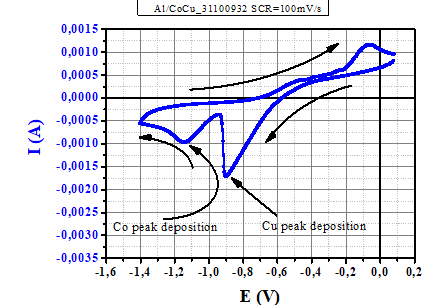
When the scan is reversed, the nucleation loop is observed. At around -0.5 V and -0.05 V an oxidation peak of cobalt and copper, respectively is detected. According to these results and the appearance of the granular thin films, cobalt deposition potential range was decided to be between -0.90 V and -1.40V. The selected potential value is Ed (Co) = -1.15V. The same was done for copper deposition potential which
was decided to be at Ed (Cu) = -0.90 V.
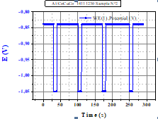
The current-time transients were also recorded to understand the nucleation and growth mechanism of cobalt films. Figure 3 shows the current-time transients of the granular thin films for the first 100 secs.
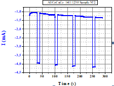
All transients show an initial increase of current due to the nucleation process. The constant current flow afterwards indicates the proper diffusion limited growth during deposition. The current value increases as the deposition times increases and the stable current value of each transient is consistent with its deposition time.
Structural characterization
The XRD patterns of cobalt/copper alloys deposited at different time: a) 500 seconds, b) 1000 seconds, c) 1500 seconds and d) 2000 seconds are shown in Figure 4. The substrate peaks of (200), (220), (220) and (311) planes which were seen at 2θ ≈ 39°, 44°, 65.5° and 78.5°, respectively are marked as S(hkl) in the patterns of the films. In the patterns, the peaks of face centered cubic (fcc) (111) and (220) planes were seen at 2θ ≈ 43° and 52°, respectively. Beside, hexagonal close packed (hcp) (10.0), (00.2) and (10.1) peaks were observed at all patterns. Under study, both phases are present; α-Co (hcp) and β-Co (fcc) in each pattern of films.
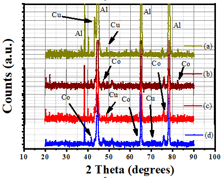
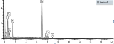
In order to clear whether there are any impurities in the prepared electrolyte or not, the ICP-AES analysis was performed. The impurities in the electrolyte can be found as an additional element in the deposits. Elemental analysis of the electrolyte disclosed that impurities in the electrolyte were found to be under the detection limits. Besides, to the compositional analysis of the deposits by the EDS, at a selected cobalt deposition time (2000 s), it was seen that pure cobalt was not only detected in the deposits. From Figure 5, the EDS spectrum of Al/(CoCu)50 sample shows that in the sample there also was some amount of impurities like carbon C according Figure 5 and the follow Table N°1.
Morphological characterization
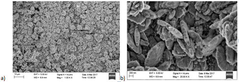
Morphology of our samples at different magnifications is shown in Figure 6. As can be seen from this Figure 6(a), at higher magnification the morphology is characterized by an almost uniform deposit composed of micro-grains. The shape of these micro-grains and their aggregation to form the light- absorbing layer is shown in the image at low magnification Figure 6(b).
| Sample Al/(CoCu)50 | Sample Al/(CoCu)25 | |||
|---|---|---|---|---|
| Elements | Wt% | Wt% Sigma | Wt% | Wt% Sigma |
| C | 6,35 | 0,8 | 6,45 | 0,84 |
| O | 14,12 | 0,39 | 8,68 | 0,33 |
| Al | 8,61 | 0,24 | 5,21 | 0,20 |
| Co | 61,92 | 0,72 | 72,08 | 0,80 |
| Cu | 9 | 0,42 | 7,59 | 0,41 |
| Total: | 100 | 100 |
Table N°1: Composition of sample Al/(CoCu)50 and Al/(CoCu)25.
The SEM pictures below, show some parallelepiped and ellipsoid shaped rods with an averaged dimension about of 600 nm length, 600 nm width and 200 nm thick for a sample electrodeposited at room temperature. These rods are irregularly arranged. Their irregular arrangement could explain the large d-spacing in the sample at this temperature. In the next step we’ll anneal the samples in order to see the effect of the temperature on the structural and magneto- optical properties of our product.
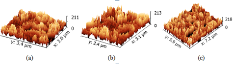
One could see that the surface of our CoCu granular thin films alloys is not smooth; it is rough as seen in Figure 7. This could be due to the roughness of the alumina surface that is not showed here. The higher thickness reached is 218 nm as can be seen in Figure 8c.
Optical characterization
Note that, we are using 300 nm-2500 nm which covers the majority of the solar spectrum. Figure 8 shows the reflectance curves of Al/CoCu granular thin films alloys stack deposited onto Alumina substrate at room temperature, which was measured using UV-Vis-NIR spectroscopy in the wavelength range of 300 – 2500 nm at different deposition time: five layers (1), ten layers (2) and ten layers (3).
As shown in the figure 8, five layers (1) reflect almost 60% in the range of 300 – 2000 nm and then increased gradually up to 2500 nm. However the reflectance drops to 20% (2), and further to 16 % (3) for the ten layers in the range of 300 – 1000 nm, which indicates that light has been absorbed in the solar spectrum region, and then both increased gradually towards the infrared region, indicating very low thermal emission in the infrared region.
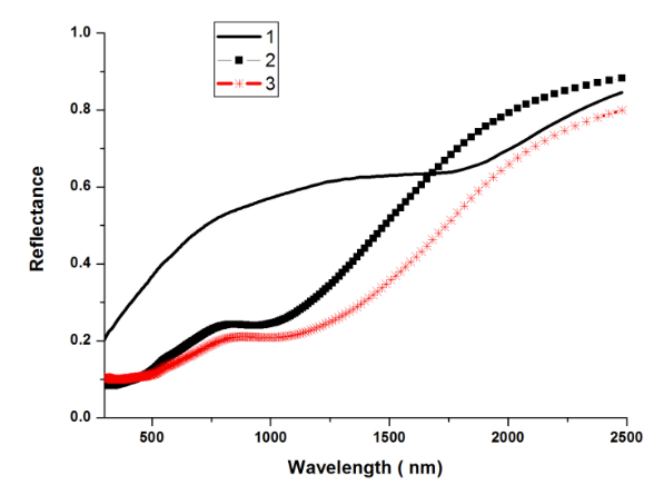
High light absorption in the solar spectrum region and low thermal emission in the infrared region are the two basic characteristics of a selective solar absorber material. Hence one can say that the Al/CoCu thin films alloys stack with five layers (1) shows high reflectance of 60% and could not be a good candidate for selective solar absorber applications. But samples electrodeposited with ten layers (2) and (3) shows lower reflectance of 20% and 16% respectively, thus making them suitable for applications in solar cells.
0.09
| d e m Field d e m | o // to the sa _1711_S1) _ 1o711_S2) _1711_S3) | d e m o mple plane (a) d e m o | d e m o d e m o | d e d e | m o m o | ||
| d e m | o | d e m o | d e m o | d e | m o | ||
| d e m d e m | o o | d e m o d e m o | d e m o d e m o | d e d e | m o m o | ||
| d e m d e m | o o | d e m o d e m o | d e m o Field // to t Al/CoCu_1 d eA lm/Co Cou_1 | d e he sampl 711_S1 711_Sd2 e | m o e plane (a m o | ) | |
| Al/CoCu_1 | 711_S3 | ||||||
| (c) d e m | o -2111S- | d e m o 1 | d e m o | d | e m o | ||||
|---|---|---|---|---|---|---|---|---|---|
| d e m d e m | o -2111S- -2111S- o | d 3 4 d | e m o e m o | d e m o d e m o | d d | e m o e m o | |||
| d e m | o | d e m o | d e m o | d | e m o | ||||
| d e m | o | d e m o | d e m o | d | e m o | ||||
| d e m | o | d e m o | Al/CoC d e mAl/ CooC | u -2111 u -2d11 1 | S-1 eS -m3 | o | |||
| d e m | o | d e m o | Al/CoC d e m o | u -2111 | S-4 | ||||
| d | |||||||||
| d e m | o | d e m o | d e m o | d | e m o |
Magnetic characterization
In figure 9 are shown in-plane and perpendicular hysteresis loops of the films produced at different deposition time.
| (b) d e m | o | d e m | o | d e | m o | d e AA | m oAAA | |||
|---|---|---|---|---|---|---|---|---|---|---|
| d e m | o | d e m | o | d e AAAAAAA | m o AA | d e | m o | |||
| d e m A | o l/CoCu | d e m _1711_S | o 1 // | A AA | d e A | m o Al/C | d e oCu_17 | m o 11_S1 | ⊥ | |
| d e m d e m | o o | d e m d e m | o o AA AA | d e A A d e | m o m o | d e d e | m o m o | |||
| d e m d e m | o o AA | d e m AA d e m | AAoAA o | d e d e | m o m o | d e d e | m o m o | |||
| A Ad e m | o | d e m | o | d e | m o | d e | m o |
Field (T)
| d e (md) | o | d e m | o | d e | m o | d | e m o | |||
|---|---|---|---|---|---|---|---|---|---|---|
| d e m d e m | o 24 24 o 24 | 11d_ Se1 m 11_S2 d e m 11_S3 | o o | d e d e | m o m o | d d | e m o e m o | |||
| d e m | o | d e m | o | d e | m o | d | e m o | |||
| d e m | o | d e m | o | d e | m o | d | e m o | |||
| d e m | o | d e m | o | d e | e1 Sm-1 o 1 S-2 | |||||
| m oAl/C Al/C | oCu -d 24 1 oCu - 241 | e1 Sm-1 1 S-2 | ||||||||
| d e m | o | d e m | o | d e | Al/C | oCu - 241 | 1 S-3 | |||
| m o | d | |||||||||
| d e m | o | d e m | o | d e | m o | d e | m o |
Magnetic results of the in-plane loops are presented in table N°2. In this table, coercivity (Hc) decreases from 48 Oe to 21 Oe whereas saturation magnetization (Ms) increases from 884 emu/cm3 to 965 emu/cm3 as the deposition time increases as shown in Fig.9. In a study [18], Hc of the Co on Cu films decreases approximately linearly with the film thickness, ranging from 192 Oe at 2.5 nm to 25 Oe at100 nm. Ms of the films are lower than the value of bulk cobalt (1422 emu/cm3 at 20 °C) [12]. Squareness (SQ), Mr/Ms also increases with the increase of deposition time. Saturation magnetization Ms increases and coercitivity (Hc) decreases which might be attributed to the deposition time as shown in the following table N°2.
For the investigation of the in-plane anisotropy in the films, as seen in figure 3, the in-plane hysteresis loop of the film (-1.0 V) has higher remanent magnetization and lower saturation field than the perpendicular one indicating the easy axis direction is in the film plane. As a result of demagnetizing effect, the shape anisotropy forces the films to have a planar easy axis. No perpendicular anisotropy has been detected for the rest of Al/CoCu films.
| Samples Name | Magnetic Properties | |
|---|---|---|
| Hc // (T) | SQ=Mr // /Ms // (%) | |
| Al/(CoCu)_2111S_3 | 0.027 | 0.053/0.177 |
| Al/(CoCu)_2111S_1 | 0.025 | 0.040/0.165 |
| Al/(CoCu)_2411S_1 | 0.033 | 0.075/0.104 |
| Al/(CoCu)_2411S_2 | 0.033 | 0.047/0.104 |
| Al/(CoCu)_2411S_3 | 0.032 | 0.35/0.077 |
| Al/(CoCu)_1811S_1 | 0.027 | 1.0E-4/0.059 |
| Al/(CoCu)_1811S_2 | 0.015 | 6.0E-4/0.025 |
| Al/(CoCu)_1611S_T | 0.024 | 0.006/0.030 |
Table N°2: Magnetic properties of the as deposited Al/CoCu multilayered granular thin films.
Conclusion
Cobalt/Copper granular thin films alloys were electrodeposited successfully in a stable and feasible bath at different deposition time between 500 seconds for copper and 3000 seconds for cobalt. All films displayed a mixture of hcp and fcc phases.
The Scanning electron microscope images (SEM) and atomic force microscopy (AFM) showed some cuboid, ellipsoid, parallelepiped and ellipsoid shaped rods with an averaged dimension about of 600 nm length, 600 nm width and 200 nm in thickness for a sample electrodeposited at room temperature. These rods are irregularly arranged. Their irregular arrangement could explain the large d-spacing in the sample at this temperature.
Saturation magnetization of the films increased and the coercivity of them decreased with the increase of deposition time. All films showed planar anisotropy. Magnetic properties exhibited a dependence on deposition time.
It was observed that the structural, magneto-optical, and morphological properties of these films are considerably affected by the deposition time and could be tailored for desired purpose [33].
Acknowledgment
One of the authors (A. Kazadi Mukenga Bantu) would like to express his appreciation and thanks to rof. M. Maaza for his valuable suggestions. Also very heartfelt thanks to all the staff members of the Materials Research Group (iThemba LABS NRF) for chemical analysis and characterization of numerous samples and for giving me the opportunity, time and facilities to complete this work.
The TWAS-UNESCO Associateship Scheme is also gratefully acknowledged for financial support which enabled this work to be carried out under the Research Project - Ref. 3240290071.
Author contributions
Conceptualization, A.K.M.B; Methodology, A.K.M.B. and M.M; Formal analysis, A.K.M.B.; Investigation, XRD-analysis and Measurements, Y. Z., N. M., L. K. and A.K.M.B.; Resources, SEM-analysis, A.K.M.B.; Writing-original draft preparation, review and editing, A.K.M.B.
Competing Interests
The authors declare no competing interests.
References
-
Jiles D (2015) Introduction to Magnetism and Magnetic Materials. Chapman & Hall UK, pp: 626.
-
Rizal C (2010) IEEE Transactions on Magnetics. 46(6): 2394.
-
Handley RC (2000) Modern Magnetic Materials, Principles and Applications. John Wiley Sons USA, pp: 768.
-
Tari S (2011) An interface study of crystalline Fe/Ge multilayers grown by molecular beam epitaxy. Applied Surface Science 257(9): 4306.
-
Diercks D, Svalov AV, Kaufman M, Vaskovskiy VO, Kurlyandskaya GV (2020) IEEE Transactions on Magnetics. 46(12): 1515-1518.
-
Soundararajan D, Mangalaraj D, Nataraj D, Dorosinskii L, Santoyo Salazar J, et al. (2009) Magnetic studies on ZnTe:Cr film grown on glass substrate by thermal evaporation method. Applied Surface Science 255(17): 7517-7523.
-
Kockar H, Alper M, Sahin T, Karaagac O (2010) Role of electrolyte pH on structural and magnetic properties of Co–Fe films. Journal of Magnetism and Magnetic Materials 322(9-12): 1095-1097.
-
Schlesinger M, Paunovic M (2010) Modern Electroplating. John Wiley & Sons Inc USA, pp: 736.
-
Karaagac O, Kockar H, Alper M, Haciismailoglu M (2012) Influence of Co:Cu ratio on properties of Co–Cu films deposited at different conditions. Journal of Magnetism and Magnetic Materials 324(22): 3834-3838.
-
Alper M, Kockar H, Sahin T, Karaagac O (2010) IEEE Transactions on Magnetics 46(2): 390-392.
-
Karaagac O, Alper M, Kockar H (2010) Characterisations of CoCu films electrodeposited at different cathode potentials. Journal of Magnetism and Magnetic Materials 322(9-12): 1098-1101.
-
Cullity BD, Graham CD (1972) Introduction to Magnetic Materials. Addison-Wesley Pub Philippines.
-
Ludwig A (2004) Combinatorial fabrication of magnetic multilayer films. Applied Surface Science 223(1-3): 78- 83.
-
Albrecht M, Ganesan S, Rettner CT, Moser A, Best ME, et al. (2003) IEEE Transactions on Magnetics 39(5): 2323- 2325.
-
Wang N, Arnold DP (2008) IEEE Transactions on Magnetics 44(11): 3696.
-
Mangen T, Bai HS, Tsay JS (2010) Structures and magnetic properties for electrodeposited Co ultrathin films on copper. Journal of Magnetism and Magnetic Materials 322(13): 1863-1867.
-
Gadwal MSM, Sartale SD, Mathe VL, Pahtan HM (2009) Substrate assisted electrochemical deposition of patterned cobalt thin films. Electrochemistry Communications 11(8): 1711-1713.
-
Cerisier M, Attenborough K, Celis JP, Van Haesendonck C (2000) Structure and magnetic properties of electrodeposited Co films onto Si(100). Applied Surface Science 166(1-4): 154-159.
-
Harti H, Bubendorff JL, Florentin A, Pirri C, Ebothe J (2011) Analysis of the substrate effect on the nucleation and growth mode of electrodeposited cobalt on copper and graphite electrodes. Journal of Crystal Growth 319(1): 79-87.
-
Szmaja W, Kozłowski W, Polanski K, Balcerski J, Cichomski M, et al. (2012) Investigation of thick cobalt films electrodeposited on gold substrates. Chemical Physics Letters, 542: 117-122.
-
Szmaja W, Kozłowski W, Polanski K, Balcerski J, Cichomski M, et al. (2012) Study of the morphological and magnetic structures of nanocrystalline cobalt films obtained by electrodeposition. Materials Chemistry and Physics 132(2-3): 1060-1064.
-
Wu H, Zei M, Yau S (2010) Journal of Physical Chemistry C114: 20062.
-
Lee JD, An TH, Noh HG, Kim SG, Choi YR (2010) Growth Kinetics and Properties of Thin Cobalt Films Electrodeposited on n-Si(100). Japanese Journal of Applied Physics 49(8): 085802.
-
Khelladi MR, Mentar L, Azizi A, Kadirgan F, Schmerber G, et al. (2012) Nucleation, growth and properties of Co nanostructures electrodeposited on n-Si(1 1 1). Applied Surface Science 258(8): 3907-3912.
-
Gao TT, Ji GB, Chang XF, Lin XH, Liu JS, et al. (2011) Electrochemical deposition and magnetic properties of cobalt and iron thin films on substrate of KIT-6/ITO. Journal of Materials Science 46: 5221-5226.
-
Rohini RP, Shubham VP, Amey MS, Kishorkumar VK, Rajanish KK, et al. (2020) Resistive Switching Memory Properties of Electrodeposited Cu2O Thin Films. J NANO ELECTRON PHYS 12(2): 02035.
-
Kiran AN , Ganesh SN, Atul CK, Tukaram DD, Tae GK (2022) Unraveling the Effect of the Water Content in the Electrolyte on the Resistive Switching Properties of Self- Assembled One-Dimensional Anodized TiO2 Nanotubes. J Phys Chem Lett 13(33): 7870-7880.
-
Bubendorff JL, Beaurepaire E, Meny C, Panissod P, Bucher JP (1997) Perpendicular magnetization in ultrathin electrodeposited cobalt films. Physical Review 56: 7120.
-
Schindler W, Kirschner J (1997) Ultrathin magnetic films: Electrochemistry versus molecular-beam epitaxy. Physical Review 55: 1989.
-
Nakahara S, Mahajan S (1980) The Influence of Solution pH on Microstructure of Electrodeposited Cobalt. J Electrochem Soc 127(2): 283.
-
Henry M, Uher J (1991)Copper plating The ground Test Accelerator RFQ. IEEE Proceedings pp: 777.
-
Lowenheim FA (1978) Electroplating. McGraw Hill Book Co New York, 6792.
-
Khadidja D, Zohir D, Ahmed B (2021) Performance Assessment of a New Gaussian-doped Junctionless ISFET: A Numerical Study. J NANO ELECTRON PHYS 13(2): 02029.
-
Somnath SK, Patil AP, Patil SL, Patil PB, Kamat RK, et al. (2022) Applied Materials Today 27: 101460.
-
Dongale TD, Khot SS, Patil AA, Wagh SW, Patil PB, et al. (2021) Bifunctional nanoparticulated nickel ferrite thin films: Resistive memory and aqueous battery applications. J Mat Des 201: 109493.
- Solution-Processed Chiral Perovskites for Biomedical Applications
- Nanotechnology in Health Chemistry and Medicine: Current Challenges and Future Directions
- Human Exposure to Micro- and Nanoplastics: Pathways, Toxicity, and Intervention Strategies
- Exosome Nanomedicine for Cancer Therapy
- Micro and Nanoplastics–Plastisphere, Biotoxicity, Impact on Human Health, and Mitigation Strategies
- Process Validation of Cefixime Powder for Suspension Dosage Form, 50 mL