Brief Review on Prospect and Applicability of Perovskite Oxide based Nonmaterial
A brief review on the prospect and applicability of perovskite oxide nanocrystal has been carried out here in this work by first of all considering different forms of perovskite oxide nanocrystal materials which often appear in powder form or as thin film form deposited on a substrate. Different deposition techniques available for use to achieve the deposition in both cases depending on the form of the material were also considered with some of these deposition methods outlined and found to be unique in its procedural approach. In this case, it was observed that some of these techniques were found to be preferred to others because of the processes involved which are often seen to offer a better atmosphere for growth of perovskite oxide material with unique structural size and morphological pattern that creates room for a better critical size and dimensions of the material that were often seen to enhance the growth of the perovskite oxide nanocrystal especially with that which possesses optimal properties that are desired for various device applications. Also, some of these applications were highlighted with the structural properties of the materials that would offer the best quality in realizing a particular application.
Introduction
Perovskite material based nanocrystals are material films with crystal structure in the form of cube with space group, the structure associated with this kinds of material is derived from the prototype CaTiO3 perovskite oxide which is general a metal oxide with the formula in which B is a small transition metal cation and A is a layer s-,d- or f- block cation. Such materials can be classified into alkaline metal halide, inorganic oxide and metal halide perovskites [1, 2, 3]. There are basically three groups of perovskite oxide based nanocrystal materials that may appear as binary, TiO3, ZnO, Al2 O3 etc: tenary, CaTiO3 BaTiO3 CaSiO3 or SrTiO3 etc. Also they may be in different forms with various types of properties and as a result they have a wide range of applications and this is more reasons and rational behind there are lots of eyes and interest on perovskite nanocrystal [4]. This is due to the numerous area of applications of the materials towards technological and energy harnessing especially in recent dispensation. These and other used of the matrteials had drawn the attention of the material science researchers over decades coupled with the vulnerability in manipulating growth materials into various application or so many other domestic usages. For instance the applications of ferroelectric, BaTiO3, PbTiO3,), dielectric (Ba,Sr)TiO3,), Piezoelectric ((Pb(ZrTi)O3), eletrostrictive (Pb(MgNb)O3), magnetoresistant, (LaCa)MnO3) and multiferric, (BiFeO3) [5, 6, 7]. had been well known especially when it comes to areas of applications with computers, memories and electronic appliances such for long such as in ferroelectric random access memories, multilayer ceramic capacitor, transducers, sensors and actuators, magnetic random access memories and other potential new types of multiple – state memories and spintronics devices that are typically controlled by electric and magnetic fields [1, 2, 3, 4, 5, 6, 7, 8]. All these varieties of applications have created quest for advancement in probing into perovskite oxide nanoscale based electronic devices that are amenable to miniaturization of conventional CMOS, complementary metal oxide semiconductor devices. These and many other reasons had led researchers in nanoscience to have the urge to focus more on the area of production and development of high volume (MLCCs) with good purity and uniform shape that would be useful in fabrication of next generation of the same MLCCs which will be of tens of nanometers for enhancement of miniaturization of the aforementioned devices.
Therefore in our review, we have observed some major challenges that were being encountered in producing these kind of materials when it comes to processing qualitative perovskite oxide on based nanocrystal materials with reliable and functional reproducible properties [9, 10, 11, 12, 13, 14], due to the complexity nature involved in the evolution processes that yields perovskite oxide materials with stiochiometry and desired properties and based on this, the fabrication and synthesis of high quality, purity, ultrafine, and agglomerated free perovskite materials with fine controlled particle size and morphology that will enhance the desired properties of the materials involve critical steps and processes would be considered, although it is clear that whichever process is used to produce the perovskite oxide material the produced material formed is found to be either in powdered form or in the form of thin film deposited on the substrate. This implies that whichever form, a specific deposition mechanism must be used. Therefore based on observed dual state in which perovikite oxide based materials can exist in and the multiple growth techniques that can be used to synthesis it, depending on state or form, the applications are enticing and as such we are poised to review its prospect and applicability.
And based on these, it is obvious that the choice of the growth mechanisms is dependent on the choice of the techniques desired which of course may be invariably determined by the availability of the equipment couple with the simplicity of the instrumental operation and control that will lead to the achievement of the necessary optimized properties which will lead to production of the perovskite nanocrystal material that would have a wide range of prospect and applicability.
Generally, the two major issues that are required to be in mind while synthesizing perovskite oxide based nanomaterials in order to achieve a desired result are (i) control of particle size and composition and (ii) the control of the interfaces and distribution of the structural blocks within the perovskite materials. However, it should be noted that the growth processes may lead to the growth of perovskite oxide nanocrystal in powder form or perovskite oxide nanocrystal in thin film form deposited on a substrate depending on the technique used. Some of these methods that may lead to grow the material either in powder or thin film form to mention but a few of them are physical vapour deposition, chemical vapour deposition electro-deposition, pulse laser, vacuum thermal, sputter deposition, successive ionic layer adsorption, hydrothermal deposition, Sol-Gel etc.
Deposition of Perovskite Oxide Nonmaterial
Since it is certain had been made known that all perovskite oxide base nonmaterial formed may be in powdered form or thin film form deposited on substrate is solely determined by the growth mechanism, there is need to highlight some growth mechanism that could be used to grow perovskite materials, therefore in this section a consideration is given to the process and growth mechanisms of perovskite oxide based nanomaterials, the growth which found to dependent on some conditions that would yield optomimum results such as simplicity, cost effectiveness, and availability of equipments and materials. Some of these processes, their basic principle and effectiveness will be highlighted here in this section.
Deposition of Perovskite Oxide Based Nanomaterial in form of Powder
Some of these techniques are based on solid- state reaction methods, molten-salt technique which involves production of powder form of perovskite material.
The first one that is solid- state method involves weighting starting materials (the corresponding oxides or oxides and carbonates), mixing, milling and calcining them at elevated temperature to form perovskite phase. For instant, in growing BaTiO3 material by solid –state reaction technique, the process involves three stages and also hinges on the diffusion of Ba2+ ions into TiO2 [15]. The first stage is the reaction with the outer surface region of TiO2 form a surface layer of BaTiO3 on the grains of TiO individually and the diffusion of Ba2+ which culminates in the formation of Ba2 TiO4 between and BaCO3 that has not been involved in reaction and the BaTiO2 as previously formed. This is followed by a prolonged sintering periods to enable the intermediate Ba rich phase Ba2TiO3 to react with the remnant of the TiO2 in the core-region of its grain to finally form BaTiO3 However, with high calcinations temperature, the agglomerated produced perovskite particle size of the powder seems to be coarse that may require further milling which may invariably result in contamination and undesirable features and defect of material.
The second one is type that uses molten salt as a medium by making use of (oxides and carbonates) [16]. The basic principle here is that it utilizes the melt-solid reaction which involves small diffusion distance with high mobility of oxides in the melt. This method is advantageous over the former one because it has one step after another; it is rapid and more environmental friendliness as regards synthesis of perovskite oxide functional materials. During the processes, it is observed that the melt increases with the rate of reaction due to small diffusion distances and high mobility of oxides in it thereby maintaining the medium of the reaction, the choice of molten salt system is variable. For instant, alkali chlorides, sulphates, carbonates, and hydroxides are the probable choices though other choices do exist. It is important to note that the feature of this technique is simple, versatile and cost effective when it comes to obtaining pure powdered perovskite materials at low temperature within a short time lapse of soaking. However the principal procedure involved in this method is heating the raw materials which includes the reactants and the salt system above melting temperature of the salt in order to enhance the synthesis of the particle at the melted salt solvent that would invariably formation of perovskite oxide powder that can be controlled by turning the heating temperature and period and after which it is allowed to cool to room temperature naturally and then it is washed with de-ionized water and then subsequently dried for it to be in complex perovskite oxide powder. This method is known to be a popular method that has been used to produce SrFeO3 nonmaterial [17] that depends on metal precursor and salt medium [18] as explained earlier.
The third technique is wet chemical methods that constitute two different techniques (a) Sol-gel colloidal process and (b) hydrothermal processes. The basic principle invoked in the main sol-gel process is formation of a sol by dissolution of metal aloxide, metal-organic ,or metal- inorganic salt precursors in a suitable solvent unlike the conventional solid- state reaction, one of the examples that are capped under this method is sol-gel colloidal process [19, 20, 21] and the other one is Hydrothermal process [22, 23, 24]. Due to its unique mechanism which involves chemical wetting solution, the dopant ions like paramagnetic or rare- earth ions can be introduced during the preparation of the solution of the precursor that will go a long way to enhances the control of the stoichiometry that invariably leads to production of narrow sized distributed perovskite materials at a low crystallization temperature. This is due to the mix at the quasi-atomic level in the solution system. One of the key concept that is imbibe this method of sol-gel is that it involves technical formation of a sol by the dissolution of the metal aloxide, meta-organic, or metal inorganic salt precursor in a suitable solvent with subsequent drying of the gel followed by calcinations and sintering at an elevated temperature to grow to perovskite crystal material. Based on these involved processes, there is homogenization at the atomic level which culminates in the considerable reduction of the diffusion distance as compared to the former methods and as such the properties of the developed crystal grown using this so-gel method has unique properties coupled with the fact that it can be used to grow the material at much lower temperatures than the former [21, 25, 26]. Optimization of developed perovskite nanocrytal can carried out by post annealing in order to affect the grain sizes of the formed perovskite oxide powder nonmaterial [27, 28, 29]. (b) In the case of hydrothermal process which is made up of two categories, conventional and microwave hydrothermal process, the process is the same although the microwave process is advantageous over conventional process due its cost effectiveness and rapid internal heating that enables the synthesis to be rapid which results from the formation of the tetragonal phase and quick increase in particle size with reaction time. However basic principle for the synthesis as applied for the duo is the same because the method involves is similar, heating an aqueous suspension of insoluble salts in an autoclave at a moderate temperature and pressure to facilitate desired phase crystallization so as to enable formation of fine and homogeneous perovskite oxide powder with good size distribution and morphology [27, 29, 30]. It has been confirmed that BaTiO3 produce using this technique has been found to formed good size distribution and morphology when it was analyzed using high resolution TEM [27].
Deposition of Perovskite Oxide Based Thin Film on Substrate
The deposition in these categories can be classified broadly into twos (i) Chemical deposition (ii) Physical deposition; the former one involves a process in which (a) the chemical precursor are directed to form on a substrate surface with the product layer growth on the surface during which the reaction is kick started. In this case the growth of the film involves heterogeneous nucleation and growth while (b) the materials are meant to dispersed into solvent either as molecular precursor or nanoparticles “ink”, or are deposited and coating formed up on the solvent evaporation and potentially annealing) and its own case, viscous fluid is deposited on the substrate. In the case of physical deposition, precipitation of vaporized material on the substrate under reduced pressure (vacuum) is firs process with the formation involving heterogeneous nucleation and growth of thin film.
Chemical Deposition Techniques includes; Chemical vapor (CVD), anodization, electroless deposition, Chemical bath deposition, CBD. Successive Ionic Layer Adsorption and reaction, SILAR, Spin/Dip Spray coating or ink jet printing of sol-gel solution or nanoparticle ink [13, 14, 15, 16, 17, 18, 19, 20, 21, 22, 23, 24] and atomic layer deposition, ALD [18, 19, 20, 21, 22, 23, 24, 25, 26, 27, 28, 29, 30, 31, 32, 33, 34, 35, 36, 37], The principle of chemical bath deposition is based in the utilization of controlled chemical reaction by ligand to induce the formation of thin film layer of a material by means of heterogeneous precipitation [38] formed from an aqueous solution of a metal salt acting as a bath for the substrate with the addition of counterion in the form of for oxides/hydroxides or for sulfides being governed by the solubility product of the target compound, and then the coating is deposited on the surface of the substrate with the required ligand to facilitated easy deposition processes [5, 2, 38]. SILAR for depositing thin film layer on the substrates operates within the combined ALD and CBD mechanism as it makes use of physically separated layer approach similar to ALD in combination with some flexibility features and CBD in conjunction with the ambient deposition technique from aqueous solutions of metal salts without the need of high- vacuum equipment [31, 32, 33, 34, 35, 36, 37, 38]. Though in contrast to CBD, it require the application of alternating baths of chemical precursors and also additional features of pure solvent in between the deposition cycles in order enable removal of excessive precursor molecules which makes its process unique such that it has the ability to deposit ultra-thin film of highly conformal coatings on a desired substrate [39, 40, 41, 42]. On the other hand it is worth mentioning here all the chemical deposition processes especially CBD and SILAR deposition techniques have a unique inherent simplicity, low cost ,effectiveness and above its ability to operate in an ambient environment which the characteristics that placed them advantageous over all the techniques used for deposition of perovskite oxide nanomaterials that are mentioned here.
Characterization of Perovskite Oxide based Nanocrystals
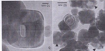
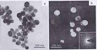
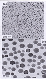
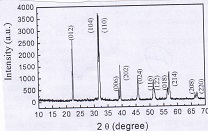
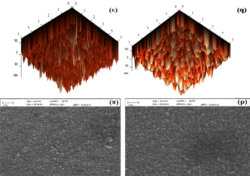
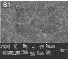
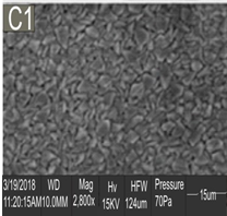
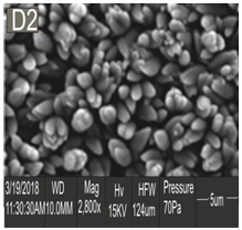
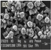
The structural characterization of the nanocrystals was carried out using TEM, HTEM, SEM and XRD. The structural features of perovskite oxide based nanocrystals in either powder form or thin film form deposited on substrate were analyzed where it was revealed that the structure of some of them like BaTiO3 powder has internal pores of various sizes have invariably effect the density of the crystals and the morphological structure of nanocrystals. However, these observed pores were seen to disappear as the material is annealed at particular temperature with formation of small particle sizes on the structure which stabilized in a cubic phase at room temperature [33, 34, 35, 36, 37, 38, 39, 40, 41, 42], a factor that is suspected to be the cause of high strain within the crystals and the reason behind the existence of structural defect within the particles ( lattice defect) because it would make the unit cell distortion ratio c/a very small than it suppose to be as that inhibits the completion of the structural transition. These are the reasons behind the variation in the contrast in the images of the morphological structure as depicted in the TEM image as shown in Figures 1-4 for powder perovskite materials while the SEM images for thin film form of the perovskite materials are shown in Figures 5-10. From the observation, there is an indication that there is a contrast variation across particles is an due to the existence of high strain in the structure must have affected the diffraction behaviour of the electrons which suggested that there might be abnormal crystallographic behaviour during the growth of the materials as indicated in the XRD pattern this may be related to the presence of strain in crystals as manifested on the morphological contrast is as shown on Figure 4 for powdered perovskite materials.
![Figure 6: SEM morphological Structure of Cu ZnO thin film [a, b, c and d] as- deposited and annealed at temperature; 500°C, 700°C and 850°C.](/fulltextimages/11547/fig_6.png)
The XRD of microwave hydrothermally powdered perovskite materials, the intensity occurred at the planes; (012), (104) and (112) while the (308) and (220) plane experienced lowest intensity as in Figure 4, but for thin film type, the highest intensity occurred at (101), (002)and (100) planes respectively as Figures 11 & 12.
![Figure 11: XRD Spectra for ZnO [1,3,5] % Al ZnO thin films.](/fulltextimages/11547/fig_11.png)
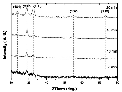
Figure12: XRD Spectra of pure and CuZnO thin film annealed at Temperatures; 500°C, 700°C and 850°C.
Recent Advances in Applications of Perovskite Oxide based Nonmaterial
Perovskite oxide based nonmaterial have been in recent time found to be indispensible essentially in modern days for some technological devices especially due to their functional properties which include Ferroelectric, Piezoelectric, Ferromagnetic dielectric, magnetoresistance, multiferroic properties that are vital to the desired optimum performance in application in various areas such as electronics, sensing, catalysis, energy harvesting, conversion and storage, optics and optoelectronics couple with the fact that some are good for passivation of layers of metals which make them to act as corrosion protection on metal surface just to mention but a few of these. It is based on this that there is now veracious quest for research on various forms and types of perovskite oxide nonmaterial using different approaches and growth mechanisms in order to ascertain the one that would enhance the improvement in optimization of the material’s applicability in industries and sciences as outlined below.
Ferroelectric and Dielectric Properties
Ferroelectric characteristics of some perovskite oxide nanomaterial such as BaTiO2 makes promising candidate for applications in thin film capacitance [42, 43, 44, 45, 46], when the structured texture and then grain sizes formed with controlled aggregation and crystal densities which lead to uniform nanocrystalline grain texture sizes while BatiO3 can be manipulated under a condition at a room temperature to possess a ferroelectric property with spontaneous electric polarization which could be reoriented by an external electric field with anticipated application on ferroelectric memories.
Magnetic Properties
The perovskite oxide nanocrystals such as BifeO3 material hinges on its particle size with emphasis on Curie temperature above room temperature for to be amenable for applications in most biomedical and magnetofluidic analysis [47, 48, 49].
Multiferroic Properties
Multiferroic characteristic of Perovskite nanocrystal is based on the coexistence of spin, orbital, and /or electric dipole order and cross-term effects between the corresponding different degrees of freedom (102,103) multiferroic and megnetoelectric characteristics of materials involve combining simultaneously ferromagnetic and ferroelectric in the same phase, with coupling between the two orders induce on it properties of spontaneous magnetization which can be reorientated by application of external electric field which is applied in magnetoelectric memory effects and magnetic switching of ferroelectric domain which is the base of in magnetic random access memory (MRAM) cell [50].
Nanoelectronics and Information Devices
Perovskite oxide nanocrystals have been of use electronic devices such as video camera, cell phone, laptop computers and automobiles because of they have a special feature in the process of multilayered ceramic capacitors (MLCC) that is very useful due to its efficiency in synthesis of electronic devices more especially for printed circuit board and hybrid circuits on ceramic substrates.
Also ferroelectric materials possess an inherent electric dielectric dipole moment in absence of an external electric field there found to have spontaneous polarization which is feature that makes such a material good candidate for random access memory, known as FeRAM (ferroelectric random access memory that could simply realized by the use of ferroelectric capacitors, in two states are normally “1” or “0” as in binary logic are represented by the manifestation of the spontaneous polarization which play vital role in electronic information. While some with good dielectric characteristics can be applied in dynamic random access memory (DRAM) which is the working medium block for information storage in the microelectronic devices that constitute the entire litany of the electronic systems.
Solar and Energy Harnessing
Optically, perovskite oxide based materials have good and effective absorption co-efficient within the visible range which is dependent on the thickness of the materials. It has been observed that within the range of some thickness, there is complete absorption of light and this makes perovskite oxide materials to exhibit good charge transfer [26, 27], which is one of the major factors that makes it favorable in solar energy harnessing and thereby indicating its prospect in solar cells conversion.
High efficiency of perovskite solar cells devices has been of interest in recent years as it efficiency is not limited only to small devices but also to large cells though the fabrication of the material with good stable and selective charge carriers extraction layers in solar cells is yet to be optimized [51, 52, 53].
Summery
In this work, we have been able to carry out a brief review of the prospect and applicability of perovskite oxide nanomaterial with consideration given to various deposition techniques that can be used to grow the materials either in powder or thin film form on a given substrate [54, 55, 56, 57]. From the review and the assessment, it was revealed that some of these deposition techniques were meant to undergoes certain unique processes during the formation of the materials that may often impact on the structural and morphological properties, especially as it concerns structural size effect of material which is found to be influential to the structural and other important properties of the materials that are discovered to be associated with a particular growth mechanisms. Also it was observed that some of these growth techniques have some added advantage over other in formation of a suitable perovskite oxide nanomaterials and then based on this it will be worthy to note that the for knowledge of this would an added advantage in making a choice in the growth mechanisms to be adopted that would help in optimizing and achieving the right critical size and dimension for the purpose of production of perovskite nanomaterials suitable for various applications while growing the material. It is clear that a better understanding of the size effects in perovskite oxide nanocrystal will be highly appreciable in making choice of the growth mechanisms that will be helpful in implementing the development of the materials amenable for various device applications. Hence, this brief review has made an attempt to assess succinctly the prospect and development of the perovskite oxide nanocrystal materials and their possible applications especially in nanoelectronics, information storage devices, and other potential application in industries. Based on these, the research on perovskite oxide based nanocrystal had found to spread like wide bush fire with thereby becoming very extensive and has thus prompting the desire to review the prospect in research of the material and their possible applications I various areas.
References
-
Chen M, Ju MG, Carl AD, Zong Y, Grimm RL, et al. (2018) Cesium Tanium(IV) Bromide Thin Film Based Stable Lead-Free Perouskite Solar cell. Joule cell Press 2(3): 558-570.
-
Chen Y, Zhang L, Zhang Y, Gao H, Yan H (2018) Large- area perovskite solar cell-a review of recent progress and issues. RSC Advances 8(19): 10489-10508.
-
Yoon DH, Lee (2002) Bi.BiFeO3 properties and powder characteristic for ceramic capacitors. J Ceramic process Res 3(2): 41-47.
-
Yoon DH (2006) Tetragonality of barium titanate powder for a ceramic capacitor application. J Ceram Process Res 7(4): 343-354.
-
Pithan C, Hennings D, Waser R (2005) Process in the synthesis of Nanocrystalline BaTiO3 Powders for MLCC. Int J Appl Ceramic Technol 2(1): 1-14.
-
Bhalla AS, Guo R, Roy R (2000) The perovskite structure-a review of its role in ceramic science and technology. Mater Res Innovat 4(1): 3-26.
-
Dawber M, Rabe KM, Scott JF (2005) Physics of thin-film ferroelectric oxides. Rev Mod Phys 77(4): 1083-1130.
-
Gruverman A, Kholkin A (2006) Nanoscale ferroelectrics: processing, characterization and future trends. Rep prog Phys 69(8): 2443-2474.
-
Hill NA (2000) Why are there so few magnetic ferroelectrics. J Phys Chem B 104(29): 6694-6709.
-
Fiebig M, Lottermoser T, Frohlich D, Goltsev AV, Pisarev RV (2002) Observation of coupled magnetic and electric domains. Nature 419(6909): 818-820.
-
Wang J, Neaton JB, Zheng H, Nagarajan V, Ogale SB, et al. (2003) Epitaxial BifeO3 Multiferroic thinnfilm heterostructures. Science 299(5613): 1719-1722.
-
Hur N, Park S, Sharma PA, Ahn JS, Guha S, et al. (2004) Electric Polarization reversal and memory in a multiferrotic material induced by magnetic field. Nature 429: 392-395.
-
Haertling GH (1999) Ferroelectric ceramics: History and technology. J Am Ceramic Soc 82(4): 797-818.
-
Moulson AJ, Herbert JM (2003) Electroceramic: Material, Properties, Applications. Jhon Wiley & Sons pp: 557.
-
Templeton LK, Pask JA (1959) Formation of BiFeO3 from BaCO3 and TiO2 in air and in CO2. J Am Ceramic soc 42(5): 212.
-
Kimaru T (2011) Molten salt synthesis of ceramic powder. In: Sikalidis C (Ed.), Advances in Ceramics- Synthesis and Characterization, processing and Specific Applications, INTECH Open Access Publisher.
-
Yang J, Li RS, Li XC, Long YL, Zhou JY, et al. (2011) Molten salt synthesis of SrFeO3 nanocrystals. J Ceramic Soc Jpn 119(1394): 736-739.
-
Li HL, Du ZN, Wang GL, Zhang YC (2010) Low temperature molten salt synthesis of SrTiO3 submicron crystallites and nanocrystals in the eutectic NaCl-KCl. Mater Lett 64(3): 431-434.
-
Frey MH, Payne DA (1995) Synthesis and processing of barium titanate ceramic from alk-oxide solution and monolithic gels. Chem Mater 7(1): 123-129.
-
Hwang UY, park HS, Koo KK (2004) Low-temperature synthesis of fully crystallized spherical BiFeO3 particles by the gel-sol method. J Am ceramic soc 87(12): 2168- 2174.
-
Brutchey RL, Mirse DE (2006) Template-free, low- temperature synthesis of crystalline barium titanate nanoparticles under bio-inspired conditions. Angew Chem Int Ed Engl 45(39): 6564-6566.
-
Dutta PK, Gregg JR (1992) Hydrothermal synthesis of tetragonal barium titanate (BaTiO3). Chem Mater 4(4): 843-846.
-
Clark I, Takeuchi T, Ohtori NC, Sinclair D (1999) Hydrothermal synthesis and characterization of BaTiO3 fine powder preursors, polymorphism and properties. J Mater Chem 9(1): 83-93.
-
Lee HS, Lee JJ, Chang TS, Kim JW, Koo SM (2007) Hydrothermal synthesis for large barium titanate powder at low temperature: effect of titania aging in an alkaline solution. J Am Ceramic Soc 90(9): 2995-2997.
-
Cho WS (1988) Structural evolution and characterization of BaTiO3 nanoparticles synthesized from polymatric precursor. J Phys Chem solids 59(5): 659-666.
-
Ciftci E, Rahaman MN, Shumsky M (2001) Hydrothermal precipitation and characterization of nanocrystalline BaTiO3 particles. J Mater Sci 36(20): 4875-4882.
-
Pinceloup P, Courtios C, Vicens J, Leriche A, Thierry B (1999) Evidence of a dissolution precipitation mechanism in hydrothermal synthesis of barium titanate powders. J Eur Ceramic Soc 19(6-7): 973-977.
-
Hertl W (1988) Kinetics of barium titanate synthesis. J Am Ceramic Soc 71(10): 879-883.
-
Hu MZC, Kurian V, Payzant EA, Rawn CJ, Hunt RD (2000) Wet-chemical synthesis of monodispersed barium titanate particles hydrothermal conversion of TiO2 microspheres to nanocrystalline BaTiO3 powder Technol 110(1-2): 2-14.
-
Eckert JO, Hung-Houston CC, Gersten BL, Lenka MM, Riman RE (1996) Kinetics and mechanisms of hydrothermal synthesis of barium titanate. J Am Ceramic soc 79(11): 2929-2939.
-
Chu MS, Rae AW (1995) Manufacturing dielectric powders. Am ceramic Soc Bull 74(6): 69-72.
-
Hu YH, Harmer MP, Smyth DM (1985) Solubility of BaO in BaTiO3. J Am Ceramic Soc 68(7): 372-376.
-
Phule P, Risbud S (1990) Low-temperature synthesis and processing of electronic materials in the BaO-TiO2 System. J Mater Sci 25(2): 1169-1183.
-
Zhou H, Mao Y, Wong SS (2007) Probing structure- parameter correlation in the molten salt synthesis of BsZrO3 perovskite submicrometer-sized particles. Chem Mater 19(22): 5238-5249.
-
Shivakumara C (2006) Low temperature synthesis and characterization of rare earth orthoferrites LnFeO3 (Ln=La, Pr and Nd) from molten NaOH flux. Solid state commun 139(4): 165-169.
-
Fossdal A, Einarsrud MA, Grande T (2004) Phase equilibria in the pseudo-binary system SrO-Fe2O3. J Solid state Chem 177(8): 2933-2942.
-
Yoon K, Cho Y, Kang D (1998) Molten salt synthesis of Lead-based relaxes. J Mater Sci 33(12): 2977-2984.
-
Chen J, Yu R, Li L, Sun C, Zhang T, et al. (2008) Structure and shape evolution of Bi1-xLaxFeO3 Perovskite microcrystals by molten salt synthesis. Eur J Inorg Chem 2008(23): 3655-3660.
-
Adewale AO, Ugwu EI, Adewale BR (2022) Influence of Ligand on the Morphological, Electrical, Optical and Solid State properties of Chemical bath Deposited PbS Thin film. Journal of Material Science Research and Review.
-
He X, Gao L (2009) Synthesis of pure phase BiFeO3 powders in molten alkali metal nitrates. Ceramic Int 35(3): 975-978.
-
Heng Wu, Xihua ZHU (2016) perovskite Oxide Nanocrystals- Synthesis, Characterization, functionality and novel applications. Open-Intech pp: 153-183.
-
Huang L, Chen Z, Wilson JD, Banerjee S, Robin son RD, et al. (2006) Barium titanate nanocrystals and nanocrystal thin films: synthesis, Ferroelectricity, and dielectric properties. J Appl Phys 100(3): 034316.
-
Park TJ, Papaefthymiou GC, Viescas AJ, Moodenbaugh AR, Wong SS (2007) Size-dependent magnetic properties of single –crystalline multiferroic BiFeO3 nanoparticles. Nano Latt 7(3): 766-772.
-
Selbach SM, Tybell T, Einarsrud MA, Grand T (2007) Sized-dependent properties of multiferroic BiFeO3 nanoparticles Chem Meter 19(26): 6478-6484.
-
Joshi PC, Desu SB (1997) Structural, electrical, and optical studies on rapid thermally processed ferroelectric BiFeO3 thin films prepared by metallo-organic solution deposition technique. Thin Solid Films 300(1-2): 289- 294.
-
Cheong SW, Mostovoy M (2007) Multiferroics: a magnetic twist for ferroelectricity. Nat Mater 6(1): 13-20.
-
Rao CNR, Serrao CR (2007) New routes to multiferroics. J Mater Chem 17(47): 4931-4938.
-
Ugwu EI (2023) Perovskite Oxide Based Thin Films Prospect and Applicability. Nanomedicine and Nanotechnology 8(3): 000240.
-
Setter N, Damjanovic D, Eng L, Fox G, Gevorgian S, et al. (2006) Ferroelectric thin films: review of materials, properties and applications. J Appl Phys 100(5): 051606.
-
Chen Y, Zhang L, Zhang Y, Gao Y, Yan H (2018) Large- area perovskite solar cells- a review of recent progress and issues. RSC advances. 8(9): 10489-10508.
-
Green MA (2001) Third generation of photovoltaic: ultra-high conversion efficiency at low cost. Progress Photovoltaic s Res Appl 9(2): 123-145.
-
Tong X, Lin F, Wu J, Wang ZM (2015) High performance perovskite solar cells. Adv Sci 3(5): 18742-18745.
-
Law C, Miseikis L, Dimitrov S, Shakya Tulahar P, Li X, et al. (2014) Performance and Stability of lead Perovskite/ TiO2 Polymer/PCBM, and dye sentized solar cell at high intensities up to 70 suns. Adv Mater 26(36): 6268-6273.
-
De Wolf S, Holovsky J, Moon SJ, Löper P, Niesen B, et al. (2014) Organometallic Halide perovskites Sharp optical absorption edge and its relation to photovoltaic performance. J Phys Chem Lett 5(6): 1035-1039.
-
Wang X, Deng LL, Wang LY, Dai SM, Xing Z, et al. (2017) Cerium oxide standing out as an electron transport layer for efficient and stable perovskite solar cells processed at low temperature. J mater chem A 5(4): 1706-1712.
-
Wang Q, Dong Q, Li T, Gruverman A, Haung J (2016) Thin Film insulating tunneling contacts for efficient and water-resistant perovkite solar cells. Adv Mater 28(31): 6734-6739.
-
Correa Baena JP, Tress W, Domanski K, Anaraki EH, Turren Cruz SH, et al. (2017) Identifying and suppressing interfacial recombination to achieve high open circuit voltage in perovskite solar cells. Energy Enviropn Sci 10(5): 1207-1212.
- Solution-Processed Chiral Perovskites for Biomedical Applications
- Nanotechnology in Health Chemistry and Medicine: Current Challenges and Future Directions
- Human Exposure to Micro- and Nanoplastics: Pathways, Toxicity, and Intervention Strategies
- Exosome Nanomedicine for Cancer Therapy
- Micro and Nanoplastics–Plastisphere, Biotoxicity, Impact on Human Health, and Mitigation Strategies
- Process Validation of Cefixime Powder for Suspension Dosage Form, 50 mL