Nanomaterials-Based Multiple Quantum Wells for High Photovoltaic Conversion Solar Cells
Using metalorganic chemical vapor deposition (MOCVD), molecular beam epitaxy (MBE) and pulse Laser deposition (PLD) techniques on GaN, Silicon, Silicon Carbide and sapphire substrates, high efficiency InGaN/GaN solar cells are reported with a particular emphasis on the work and achievements made with multi-junction tandem and Nanomaterials (Quantum well (QW), Multiple Quantum Wells (MQW), and Quantum Dots (QD)). An effective method for increasing photon absorption in ultrathin cells made for the best possible photovoltaic response is the InGaN/GaN QW system. To maximize light absorption, the quantum well and barrier thicknesses and number of wells in the MQW active region must be adjusted.
Introduction
The use of fossil fuels for transportation and industrial processes contributes to global warming. Wind turbines and photovoltaic solar cells are two examples of renewable energy sources that work well in windy or sunny regions. To speed up their evolutionary process, developing nations in particular must expand their terrestrial and spatial influence areas (space, desert, sea, mountains, etc.). These nations are investing more and more on research and development, which needs to be concentrated in a particular field based on their available financial and people resources. The multilayer construction of the third generation of solar cells allows them to theoretically achieve an energy conversion efficiency of about 86%, which is about three times higher than the
31% theoretical value of one junction in currently available silicon-based commercial cells. Recent technological advances have led to an excessive amount of complicated structures and novel materials incorporating several systems and parameters that need to be studied. Group-III nitride elements are appealing because materials such as GaN or InN exhibit stability and robustness under harsh temperature and radiation regimes. The insertion of low-dimensional systems like quantum wells (QW), quantum wire wells (QWW), and quantum dots (QD) in the intrinsic region of a standard p-i-n photodiode has been made possible in the last few years by the mastering of Nanomaterials using different experimental techniques such as MOVPE, MOCVD, BEM, etc.. By introducing other carrier levels in solar cell band gap, this method creates an accessible energy band that allows photons with energy below the band gap to be absorbed. In conventional solar cells, this photon category—which makes up the most significant components of power loss in single band gap solar cells—would typically not be absorbed or lost as heat. In this sense, during the past few decades, we have studied the effects of different profiles (rectangular, parabolic, and triangular) for single and multiple QW, accounting for the effects of heavy holes and impurities as well as the temperature stability of based devices [1, 2, 3, 4, 5, 6].
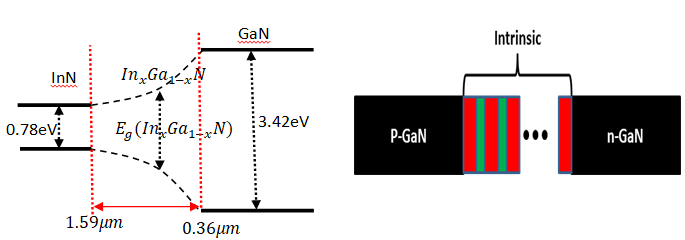
Infrared (IR) photodetectors are an interesting topic because of their numerous existing and future uses in the industrial, scientific, and military domains. Innovative materials like (In,Ga)N ternary, in addition to conventional silicon material, may be a good option for getting additional refunds, even though production technology is still a complicated and costly alternative. Due to their exceptional photovoltaic characteristics, tunable band gap energies, and physical and chemical stabilities, (In,Ga)N alloys have lately become interesting materials [7, 8, 9, 10, 11, 12, 13]. In addition, because of the possibility of their applications in ultrafast optoelectronic parts like all optical switches for optical networking systems, near-infrared photodetectors, and quantum cascade lasers, intersubband transitions (ISBTs) in semiconductor quantum wells and their associated optical absorption have drawn attention from researchers in recent years [14, 15]. The main parameter governing the optical absorption is the band gap energy of the ternary (In,Ga)N which depend nonlinearly on the In-content as reported on Figure 1.
The PV conversion efficiency of the multiple junction PV cells [16, 17, 18, 19] and the tandem PV cells [20, 21, 22] are better than the one of the single-junction cells (Table 1).
| Number of Junctions | Optimum Band Gaps (eV) | Efficiencies (%) | |||
|---|---|---|---|---|---|
| Eg1 | Eg2 | Eg3 | Eg4 | ||
| 1 | 1.31 | - | - | - | 31 |
| 2 | 0.98 | 1.88 | - | 42.7 | |
| 3 | 0.83 | 1.45 | 2.26 | - | 49.1 |
| 4 | 0.73 | 1.23 | 1.78 | 2.56 | 53 |
| ∞ | - | - | - | - | 69 |
| ∞ (w/conc.) | - | - | - | - | 86.8 |
Table 1: The maximum (Ideal) theoretic efficiencies for solar cells with the number of junctions based on the thermodynamic appro
Issues and Major Obstacles to High Nitrides Conversion Efficiency
To fully realize the promise of III-nitrides in high frequency radiofrequency and optoelectronic components, a number of obstacles must be addressed. Lattice mismatch between InN and GaN: this effect induces nonradioactive recombination centers produced by impurity incorporation and morphological defects. However, carrier lifetimes are decreased by such centers in solar cells.
High Indium Content in InGaN Ternary: This is necessary for an efficient conversion of lower energy photons; nevertheless, this necessitates a thick layer and decreases its light absorption. Additionally, the management of polarization will get more difficult when InGaN solar cells move toward larger Indium concentrations ( ) 30% ≥ to increase the spectral sensitivity to longer wavelengths, which tends to the polarization-induced electric fields showing high threading dislocation (TD) densities in the
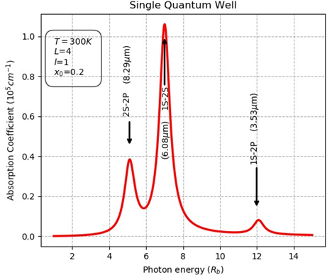
8 10 2 10 10 cm− − range. The conversion efficiency gets reduced as a result. The photogenerated carriers recombine with the defect states before they reach the electrodes, resulting in low efficiency caused by the short diffusion length of the carriers caused by the high density defects. Phase separation in InGaN films is easily induced by Indium (In) rich clusters when the thickness and/or mole fraction of materials rise which results in poor fill factor (FF), higher recombination rate by defect states, and lower open-circuit voltages (VOC) relative to theoretical values, all of which reduce the short- circuit current density (JSC) of InGaN-based PV devices. Dielectric Mismatch: This effect induces a built in-electric field at the InGaN/GaN interfaces augmenting the threading dislocation density which reduces the PV conversion efficiency. Heteroepitaxy: Nowadays, it is still difficult to develop high quality InGaN epitaxial layers on GaN with thicknesses more than 100_nm_ and band gaps smaller than 2_eV_ . Absorption: The near UV to far-infrared areas of the absorption spectra of InGaN material offers a strong promise for PV applications. Increasing the In-composition causes the absorbance of photons with low energies, which is advantageous for P-I-N-based SC. To get shine on such important parameter, we present in Figure 2 the obtained results for 0.2 0.8 In Ga N GaN QW in which three first low-lying states are implied (1S, 2S and 2P). The results are obtained using the numerical finite difference method to solve the Schrodinger equation coupling to Poisson equation taking into account of different parameters like, band gap narrowing, segregation, polarization and so…. It is clearly seen that the main intersubband transition is located at 6.08 m µ while the second and the third are located respectively at 3.53 m µ and 8.29 m µ . It is interesting that these values and their corresponding amplitudes can be controlled by adjusting internal and external parameters such as: In-content, thickness, temperature, pressure, and so on.
In order to improve the PV conversion efficiency, MQWs are the promising candidate to overcome the Shockley- Queisser limit. Table 2 illustrates the reported results concerning the MQWs-based solar cell.
| Solar cell MQWs performance | In content in InGaN | External Efficiency |
|---|---|---|
| In Ga N GaN x 1−x | x =3% | 50% [23] |
| x =12% | 72% [24] | |
| x =28% | 69% [25] | |
| x =14% | 60% [26] | |
| x =60% | 20% [12] |
Table 2: PV performance of 0.2 0.8 _In Ga N GaN_ solar cell-based MQWs obtained on sapphire substrate under AM1.5G illumination.
Considerable advancements have been achieved in the fundamental comprehension and engineering techniques pertaining to InGaN-based solar cells. Fundamental understanding has grown in the areas of carrier dynamics at high temperatures, polarization effects, loss processes, and carrier transports. At the device level, techniques for fabricating devices and materials epitaxy were taken from the established InGaN LED technologies. InGaN-based non- polar m-plane solar cells with quantum yields above 80% at 450 °C have been established as a result of these efforts; such a performance has never been observed on other solar cell material architectures. Even with these optimistic developments, more advancements in components, devices, and integrating strategies remain essential to surpass the PCE limit of the present generation of InGaN-based solar cells and enable their use in more practical contexts [23, 24].
Conclusion and Perspective
Recent advancements in the area of photovoltaic cells based on III-nitride semiconductors have been covered in this piece of work. Because of their direct and adjustable band gap and great dependability, III-nitride semiconductors are an excellent choice for a wide range of electrical and optoelectronic applications, including high efficiency solar cells, brilliant LEDs, and laser diodes [25, 26]. The functionality and dependability of the final device are impacted by a multitude of critical material qualities that are determined by the substrate selection. Integrating InGaN- based solar cells, with currently available multijunction solar cells like Si, GaAs-based III-V and perovskites solar cells, is the best solution in order to get efficiencies greater than 50%. Nevertheless, when it comes to epitaxial growth, InGaN materials are incompatible with others like Si and GaAs. In order to generate electrically coupled InGaN/ III-V/Si multijunction solar cells, novel approaches to wafer adhesive and solar cell incorporation need be investigated. These developments will hasten the deployment of InGaN- based solar cells in more practical settings. With the right polarization and band engineering, cautious device design, and modeling before manufacture, excellent performance and low cost solar cells can be achieved.
References
-
Ghazi HE, Ramazan YE, En nadir R (2024) Numerical Analysis of InGaN/GaN Intermediate Band Solar Cells Under X-sun Concentration, In-compositions, and Doping: Unlocking the Potential of Concentrated Photovoltaics. Arab J Sci Eng.
-
Abboudi H, El Ghazi H, Benhaddou F, En-Nadir R, Jorio A, et al. (2022) Temperature-related photovoltaic characteristics of (In,Ga)N single-intermediate band quantum well solar cells for different shapes. Physica B Condensed Matter 626: 413495.
-
Abboudi H, EL Ghazi H, En-nadir R, Basyooni MKMA, Jorio A, et al. (2024) Efficiency of InN/InGaN/GaN Intermediate-Band Solar Cell under the Effects of Hydrostatic Pressure, In-Compositions, Built-in-Electric Field, Confinement, and Thickness. Nanomaterials 14(1): 104.
-
En nadir R, El Ghazi H, Jorio A, Zorkani I, Kilic HS (2022) Intersubband optical absorption in (In,Ga)N/GaN double quantum wells considering applied electric field effects. J Comput Electron 21(1): 111-118.
-
En nadir R, Basyooni MKMA, Tihtih M, Belaid W, Ez Zejjari I, et al. (2023) Enhancing Emission via Radiative Lifetime Manipulation in Ultrathin InGaN/GaN Quantum Wells: The Effects of Simultaneous Electric and Magnetic Fields, Thickness, and Impurity. Nanomaterials 13(21): 2817.
-
En nadir R, El Ghazi H, Leontie L, Tihtih M, Zaki SZ, et al. (2023) Tailoring optoelectronic properties of InGaN-based quantum wells through electric field, indium content, and confinement shape: A theoretical investigation. Physica B Condensed Matter 663: 414976.
-
Walukiewicz W, Ager JW, Yu KM, Weber LZ, Wu J, et al. (2006) Structure and electronic properties of InN and In-rich group III-nitride alloys. J Phys D Appl Phys 39.
-
Wu J (2009) When group-III nitrides go infrared: New properties and perspectives. J Appl Phys 106: 011101.
-
Farrell RM, Neufeld CJ, Cruz SC, Lang JR, Iza M, et al. (2011) High quantum efficiency InGaN/GaN multiple quantum well solar cells with spectral response extending out to 520 nm. Appl Phys Lett 98: 201107.
-
El Ghazi H, Jorio A (2014) Temperature dependence of interband recombination energy in symmetric (In,Ga) N spherical quantum dot-quantum well. Physica B Condensed Matter 432: 64-66.
-
Belghouthi R, Salvestrini JP, Gazzeh MH, Chevelier C (2016) Analytical modeling of polarization effects in InGaN double hetero-junction p-i-n solar cells. Superlattices and Microstruct 100: 168-178.
-
Belghouthi R, Taamalli S, Echouchene F, Mejri H, Belmabrouk H (2015) Modeling of polarization charge in N-face InGaN/GaN MQW solar cells. Mater Sci Semicond Process 40: 424-428.
-
Lourassi M, Soudini B (2016) Simulation of piezoelectric and spontaneous polarization effect on the InGaN/Si tandem solar cell. Optik 127(5): 3091-3094.
-
En nadir R, El Ghazi H, Belaid W, Jorio A, Zorkani I, et al. (2021) Ground and first five low-lying excited states related optical absorption in In.1Ga.9N/GaN double quantum wells: Temperature and coupling impacts. Solid State Communications 338: 114464.
-
En nadir R, El Ghazi H, Jorio A, Zorkani I (2021) Ground- state Shallow-donor Binding Energy in (In,Ga)N/GaN Double QWs Under Temperature, Size, and the Impurity Position Effects. J Mod Sim Mater 4(1): 1-6.
-
Li Z, Xiao H, Wang X, Wang C, Deng Q, et al. (2013) Theoretical simulations of InGaN/Si mechanically stacked two-junction solar cell. Phys B Condens Matter 414: 110-114.
-
Bhuiyan AG, Sugita K, Hashimoto A, Yamamoto A (2012) InGaN solar cells: Present state of the art and important challenges. IEEE J Photovoltaics 2(3): 276-293.
-
Zhang X, Wang X, Xiao H, Yang C, Ran J, et al. (2008) Theoretical design and performance of InxGa1-xN two- junction solar cells. J Phys D Appl Phys 41(24).
-
El Gmili Y, Orsal G, Pantzas K, Moudakir T, Sundaram S, et al. Multilayered InGaN/GaN structure vs. single InGaN layer for solar cell applications: A comparative study. Acta Mater 61(17): 6587-6596.
-
Hsu L, Walukiewicz W (2008) Modeling of InGaN/Si tandem solar cells. J Appl Phys 104: 024507.
-
Hamzaoui H, Bouazzi AS, Rezig B (2005) Theoretical possibilities of InxGa1-xN tandem PV structures. Sol Energy Mater Sol Cells 87(1-4): 595-603.
-
Martí A, Araújo GL (1996) Limiting efficiencies for photovoltaic energy conversion in multigap systems. Sol Energy Mater Sol Cells 43(2): 203-222.
-
Lee YJ, Lee MH, Cheng CM, Yang CH (2011) Enhanced conversion efficiency of InGaN multiple quantum well solar cells grown on a patterned sapphire substrate. Appl Phys Lett 98: 263504.
-
Neufeld CJ, Cruz SC, Farrell RM, Iza M, Keller S, et al. (2007) Observation of positive thermal power coefficient in InGaN/GaN quantum well solar cells. Appl Phys Lett 99: 071104.
-
Matioli E, Neufeld C, Iza M, Cruz SC, Al Heji AA, et al. (2011) High internal and external quantum efficiency InGaN/GaN solar cells. Appl Phys Lett 98: 021102.
-
Shiming L, Quan W, Hongling X, Kun W, Cuimei W, et al. (2017) Optimization of growth and fabrication techniques to enhance the InGaN/GaN multiple quantum well solar cells performance. Superlattices and Microstructures 109: 194-200.
- Solution-Processed Chiral Perovskites for Biomedical Applications
- Nanotechnology in Health Chemistry and Medicine: Current Challenges and Future Directions
- Human Exposure to Micro- and Nanoplastics: Pathways, Toxicity, and Intervention Strategies
- Exosome Nanomedicine for Cancer Therapy
- Micro and Nanoplastics–Plastisphere, Biotoxicity, Impact on Human Health, and Mitigation Strategies
- Process Validation of Cefixime Powder for Suspension Dosage Form, 50 mL