Thriving Perspectives of Nanotechnology: A Review
Most of us may erroneously accept that sciences inside the nanosystems are a basic expansion of what is seen in the μm scale, this perception is amiss. In a generous way and with the trendy interpretation one can define nanotechnology as a science which is having its significance at the nanoscale, but deep inside this definition, there is an entire universe of opportunities and innovations which can be very helpful in solving numerous present and future challenges in assorted domains such as environment, sustainability, technology advancement, medical, engineering, etc. In this review, a concise introduction to nanotechnology is given including the origination and different prospects of nanotechnology in the first part followed by the application-based opportunities and recent work in various fields.
Prachi Soni1, Gagan Kant Tripathi1*, Shashank Saurav1, Purnima Swarup Khare1 and Murthy Chavali2,3
Introduction
Nanotechnology is a science which is actualized at the nanoscale and had applications in a substantive world [1, 2, 3]. Nanotechnology can also be characterized as a science and engineering which implicates the design, synthesis and characterization of materials at the nanoscale or one billionth of a meter [2, 3, 4]. Nanostructures are broadly defined in the range of 1-100nm. Briefly, we can interpret nanotechnology as ‘atomically precise technology’ or ‘engineering with atomic precision’ [3, 4, 5]. Nanotechnology became famous worldwide and gains scrutiny due to its potentially strong technological background and application in commercial devices.
Nanotechnology is having the capability and dynamism to resolve global issues. It is impressive to know that as the size of the particle reduces to the nano range, there are a lot of variations appeared in the different properties (magnetic, ferromagnetic, catalytic, electrical, mechanical, optical, etc.) of the material. It was first conceptualized by physicist Richard Feynman in 1959. Nanotechnology is the ability to recognize, monitor and manipulate material at the level of individual atoms and molecules, according to the National Science Foundation [4, 5, 6, 7, 8, 9, 10, 11, 12, 13]. Nanotechnology being a sub-branch of science is expanding itself as a multidisciplinary field in and having applications in domains such as engineering, bioengineering, electronics, medicine, pharmaceuticals, etc). It is also looming as a new technology which provides a solution for environmental challenges such as safe and clean renewable energy, water treatment, etc.
Various advancements in the materials as nanomaterials which are having admissible properties as well as high-end engineering applications are also shown as the emergence of nanotechnology [5, 6, 7, 8, 9, 10, 11]. There are many nanomaterials, few of them are naturally occurring and some are artificially engineered and synthesized according to the requirement. The synthesis techniques for nanomaterials broadly classified into 2 types i.e. top-down synthesis technique and bottom-up synthesis technique.
Among these two techniques, the bottom-up technique is preferable because of its accuracy and ability to make a more precise structure. In this review, nanotechnologies in various fields and industries have been discussed keeping the eye on the future advancements, also the advanced synthesis techniques for the synthesis of nano range structures is discussed.
Impact of Nanotechnology on Various Fields
In recent year nanotechnology has become a very common term to not only among the researchers but also among the industrialists and tech persons. Nanotechnology is a branch of engineering which uses nanoscience to play at the nanoscale and accord variety of useful products with novel properties and size. The field of nanotechnology not only stretching itself in medical, material science, biology, chemistry, pharmaceuticals but also in the area of advanced manufacturing methods, water purification systems, engineering, resolving environmental issues, nanomedicine, cancer treatments and also developing better food production methods and agriculture essentials that contain a high amount of nutrients. The reduced size of the material enhances its properties that in every field we can able to play with the smallest and unreachable dimensions of the materials. With the help of this potential, discoveries of new material are also going on. The development in the field of nanotechnology was started in 1959, and since then various advancements have been taking place in this field [3, 4, 5, 6, 7, 8]. There are many materials developed in the field of nanotechnologies such as Graphene, Carbon Nano Tube (CNT), Nanowires, Quantum dots, Nano powders, Fluorescent Nano-diamonds, Nano clays, and structures such as mesoporous structures, dendrimers, etc.
There is also several risks of nanotechnology, in terms of environmental issues, health, safety and social issues. Some of the nanomaterials are not suitable for the environment and life cycle assessment (LCA) investigation is required and also there is no floor test accepted for the recyclability of the nanomaterials till now [6, 7, 8, 9]. Nanotechnology implies to be a most futuristic, young and dynamic technology that impacts the economic growth of the world and has the potential to invent numerous employment opportunities in conjunction with the great space for innovation and research [7, 8, 9, 10]. Figure 1 shows periodical growth in the field of nanotechnology.
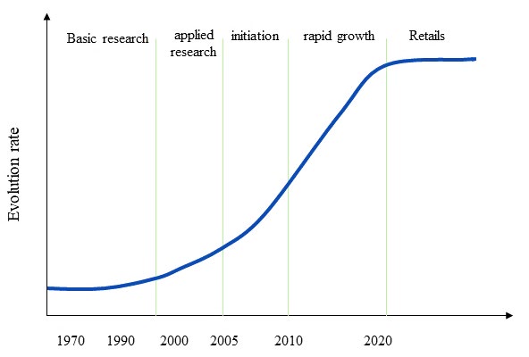
Nanotechnology has built up a quarter of a trillion dollars worldwide market since 2009, becoming such a general- purpose technology by 2020 by covering four generations of more structurally and dynamically ramified products, i.e. 1) Passive nanostructure, 2) Active nanostructure, 3) Nanosystems, and 4) Molecular nanosystems [8, 9, 10, 11, 12]. Figure 1.Presents the span-based surge in the field of nanotechnology in terms of its stages.
History of Evolutions in Nanotechnology
- In the year 1959, it was all started with the lecture on ‘There’s a Plenty of Rooms at the Bottom’ by physicist Richard Feynman in American physical society at Caltech, where he gives the initial idea about nanotechnology by the insight miniaturization of things [9].
- In 1974, just about 15 years after Feynman’s talk, a Japanese researcher, Norio Taniguchi, was the first to utilize the term ‘’nanotechnology’’ to represent semiconductor processes at the nanoscale [10].
- In 1981, IBM developed a Scanning Tunnelling Microscope. STM was invented by two of the greatest physicists of IBM, GK Binnig and Heinrich Rohrer in 1981. For this invention, they both were awarded a Nobel Prize in Physics in 1986. This invention plays a major role in the field of nanotechnology. This invention permitted the scientists to see the world’s first image of individual surface atoms and the bonds that hold them in place by the help of STM [11].
- In 1985, first nanoparticles, Bucky balls were discovered. Bucky balls which are also known as the name’s fullerene were discovered by the researcher’s trio Richard Smalley, Harry Kroto and Robert Curt, at the Rice University. The structural arrangements of Bucky balls are such that carbon atoms linked to three other carbon atoms by covalent bonds. Due to this covalent bond between the carbon atoms, Bucky balls are very strong. The most common Bucky balls contains 60 carbon atoms and hence sometimes it is also called as c60 [12, 13, 14].
- The year 1986 brought an extensive revolution in the field of nanotechnology. It was that year when the Atomic Force Microscope (AFM) was first invented by Gerd Binnig, Calvin Quate and Christoph Gerber in 1986, then speculated about the possibility of achieving atomic resolution. This resolution technique, AFM is the most helpful tool for imaging, measuring and also for manipulating matter [13].
- IBM logo made with individual atoms in 1989. Don Eigler, an IBM physicist, became the first person to manipulate and position individual atoms on 28 September 1989. He arranged 35 Xenon atoms, one and a half months later, to spell out the letters IBM. At that time, it took around 22 hours to write those three characters. Nowadays it takes just 15 minutes [14].
- In 1991, carbon nanotubes (CNTs) were discovered by Iijima. This revelation offers rise to the new part of material science i.e. Nanoscience. This disclosure also sights the fourth state of matter i.e. It has been found that water trapped inside a carbon nanotube, which does not act either as gas, liquid or solid. CNT is going to play a massive role in the future in various fields [15, 16, 17, 18].
- In the year 1999, one more step was taken in the field of nanotechnology. First nanomedicine book named “Nanomedicine” by R. Freitas was published. This book tends to the specialized issues associated with the medical utilization of molecular nanotechnology and medical nanodevice design [16].
- First National Nanotechnology Initiative program (NNI) was launched in 2000 by the United States. These programs give new opportunities in the field of nanoscale science, engineering and technology [17].
- Feynman Prize in Nanotechnology was awarded in 2001.
Mark A Ratner, Professor of Chemistry at Northwestern University, was awarded for the development of electronic devices on a nanometer scale theory. Their research has significantly contributed to the production and performance of electronic devices on a nanometer scale. For their experimental research, which included pioneering contributions to the synthesis and characterization of particular physical properties of carbon nanotubes and nanowires, Professor Charles M. Lieber (Professor of Chemistry), Harvard University was awarded [18].
Nanomaterials
A material which is having its external dimension or internal structure or surface structure dimension in nanoscale is considered to be a nanomaterial [18] although nanoparticle (NP) can be construed to have at least one of its external dimensions in nanoscale i.e. 1-100nm. According to the European agencies, ‘nanomaterial’ term can be defined in the following way [19].
‘Nanomaterial’ means a normal, incidental or manufactured substance containing particles in an unbound state or as aggregate or as an agglomerate and where one or more external measurements are within the size range 1–100 nm for 50% or more of the particles in the number size distribution. The number size distribution threshold of 50% can be replaced by a threshold between 1 and 50% in particular cases and where economic, health, safety or competitiveness considerations warrant. The fullerenes, graphene flakes and single-wall carbon nanotubes with one or more external dimensions below 1 nm should be known as nanomaterials by derogation from the above definition [12, 13, 14, 15, 16, 17, 18].
Classification of Nano Materials
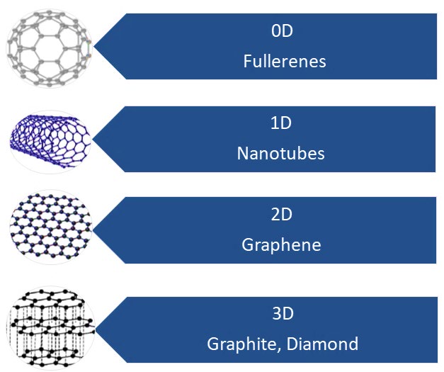
The diversity of nanomaterials can be classified based on their dimensionality [20]. In the classification of nanomaterials based on their dimensionality can be defined as the number of dimensions of the nanomaterial which are outside or inside the nanoscale range i.e. between 1-100nm. Figure 2 shows a schematic illustration of the dimensions of the nanomaterials.
- Zero Dimension Nanomaterials (0D) which are purely considered as NP as all the dimensions are within the range of 1-100nm i.e. no dimension is greater than 100nm.An example of 0D includes quantum dots, fullerenes, etc.
- One Dimensional Nanomaterials (1D) are generally those which have their one of the dimensions out of the range of nanoscale or greater than 100nm and the other two dimensions are in the nanoscale range. These groups of nanomaterials are generally including nanotubes, nanowires, nanorods, etc.
- Two Dimension Nanomaterials (2D) are classified as having their two of the dimensions out of the 1-100nm range. This type of nanomaterials is generally in the form of plates and includes nanomaterials like graphene, nanosheets, nano-thin films, nanolayers, and nano- coatings.
- Three Dimensions Nanomaterials (3D) are those which do not have any of the dimensions which are confined to the scale of 1-100nm.
All the dimensions in this type of nanomaterials are outside the range of 1-100nm. This can include bulk powder, dispersion of NP, bundles of nanowires and nanotubes and nanorods.
Utilization of Nanotechnology
Thin Films
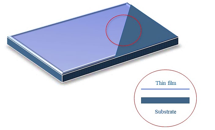
Nano thin films can be characterised as having a thickness of a material layer in nanometres i.e. ranging from 1-100nm. There are several processes for the synthesis of thin films such as vapour deposition methods like chemical vapour deposition (CVD) and physical vapour deposition (PVD), Electrodeposition, Lithography technique, pulse laser deposition (PLD), sol-gel method and so on. There are many nanoparticles which can form thin films which give them special properties like anti-reflective glass, anti-fog property, water repellent property, scratch-resistant, anti-microbial property, conductive films, etc. Figure 3 shows Thin Film example on the substrate. The act of applying a thin layer of a substance on to a surface/substrate is called thin film. Based on the nature of deposition processes and methods employed for thin film deposition are categorized into two groups. Figure 4 shows the respective chart is showing the various modes used for the thin film [21, 22, 23, 24].
Physical Thin Film Deposition: Physical deposition uses mechanical or thermodynamic means to produce a thin film of solid. Since most engineering materials are held together by relatively high energies, and chemical reactions are not used to store these energies. Commercial physical deposition systems tend to require a low-pressure vapour environment to function properly. Some of the commonly used physical methods are vacuum evaporation, molecular beam epitaxy, pulsed laser deposition, reactive evaporation, cathode arc deposition, diode sputtering, plasma-enhanced evaporation, reactive sputtering, and magnetron sputtering etc [24, 25, 26, 27, 28].
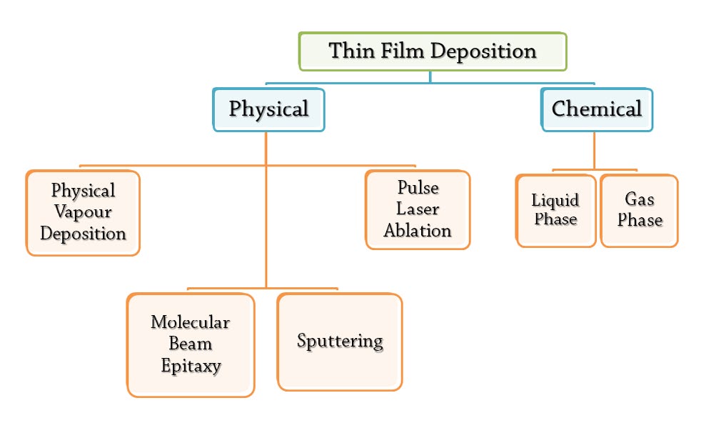
Chemical Thin Film Deposition: Chemical deposition uses a fluid precursor undergoes a chemical change at a solid surface, leaving a solid layer. Chemical solution depositions use a liquid precursor, usually a solution of organ metallic powder dissolved in an organic solvent. This is a relatively inexpensive, simple thin-film process that can produce stoichiometrically accurate crystalline phases. Figure 5 shows Different Chemical Methods for films deposition.
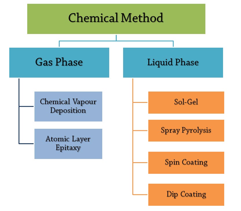
Some of the commonly used chemical methods are Chemical vapour deposition, spray pyrolysis (SPT), Electrodeposition, Dip growth, Successive ionic adsorption and reaction (SILAR), Chemical bath deposition (CBD), Co- precipitation, Spin coating, Sol-gel etc. Out of all deposition techniques, it is now established that the chemical techniques can produce smooth, uniform and adherent intermetallic films. In the present work we have, therefore, used a simple homemade chemical Spray Pyrolysis Technique for the preparation of nanocrystalline thin films.
Nano Electronics
Make electronic devices size within nanometers range. In the activities of these nano-electronic instruments, interatomic interactions and quantum mechanical properties assume a significant task. Some quantum effects, such as tunnelling and atomic disorder, characterize these nano- electronic devices’ characteristics [21]. Nanotechnology has the power to reshape the electronics industries from top to bottom. Nanotechnology can offer us:
- Uniform size and structures of nanomaterials like in metal, oxides, ceramics and composites;
- Reactive particles advantages due to the large surface area in metals, oxides, ceramics and composites;
- Extraordinary optical, magnetic, thermal, electrical and electronics properties like in phosphors, heat pipes, percolation-based conductors;
- Nanostructured materials such as nanotubes, nanowires, electrodes, thin films, etc [22].
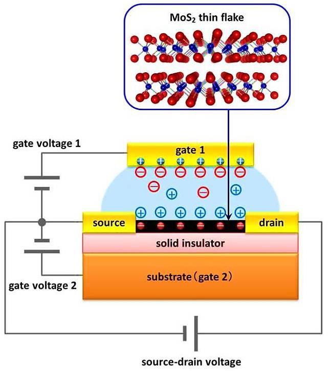
One of the most focussed areas in the nanoelectronics is the transistors. According to Moore’s law “the number of transistors per square meter on a microchip doubles in every two years, though the cost of the computers is halved”. This statement clears that the size of the transistor is getting smaller and smaller day by day due to the advancements in the nanotechnology; simultaneously the power consumption of the computer is becoming less and the capacity of the device is getting increased. There are lots of works going on to reduce the channel length of the transistor. Presently, the estimated channel length for the molybdenum disulphide (MoS2) through CVD synthesis is down to 20 nm [23]. The smallest working transistor today is 7nm long [21, 22, 23, 24, 25, 26], and lots of work are going on 5nm transistor technology. Other than transistors, nanoelectronics also has its application in various other fields like, spintronics (a device which is used as a memory for data storage), displays, wearable and flexible gadgets, optoelectronics, energy devices, etc. Figure 6 shows the MoS2 nanosheet nano-transistor.
Medical
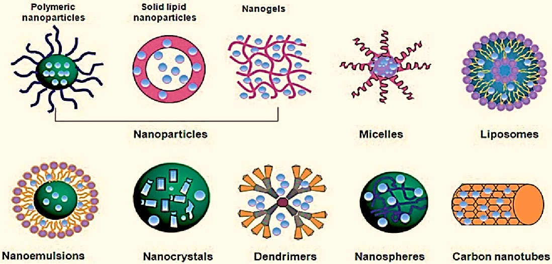
Drug Delivery: Nanotechnology makes the drug delivery inside the body very precise and accurate. With the help of targeted drug delivery, it reduces a lot of complications and side effects during the treatment of various severe diseases such as cancer. There are several nano-materials which make it feasible. Some main nano-materials which play a significant role in drug delivery are liposomes, dendrimers, nanoshells, polymer micelles, lipids; metallic nanoparticles such as Au NP; nanocrystals and quantum dots. Such materials have a high degree of biocompatibility for different functions before and after conjugation with biomolecules to turn into nanomedicines and clinical practice [24]. Figure 7 representation of a targeted drug delivery system through nanocarriers.
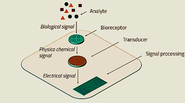
Biosensors: Biosensors are the devices which use different nanomaterials like gold nanoparticles, silver nanoparticles, zinc nanoparticles, etc for the detection of different organic analytes such as, a biomolecule, any microorganism or any biological structure. With the help of a biosensor, the presence, as well as the concentration of the analyte, can be detected. A biosensor mainly consists of three main parts i.e. a sensor which detects the targeted analyte, a transducer which converts the detected signal into readable output and a reader device through which we can read the information given by the sensor [25, 26, 27, 28, 29]. Figure 8 shows a schematic representation of the structure of biosensor. There are various types of biosensors in working presently and many are under research and development. The most common types of biosensors are piezoelectric biosensor, optical biosensors, electrochemical biosensors, thermometric biosensor, etc. Biosensors have several applications such as insulin detection, cancer detection, metabolites measurements, ecological pollution monitoring, diagnosis of diseases, agriculture, etc.
Pharmaceuticals: Nanotechnology is very progressive in the field of medicines. With the superiority of nanomaterials to interact as the reduction of size to the nanometer scale, it is becoming key to many challenges and broadens the area of research in the biological field [26, 27, 28, 29, 30, 31]. Even today several diseases like diabetes, cancer, etc are imposing severe illness to mankind. Nano-medicine can interact at the molecular level can help in fast recovery of the disease, also the side effects can be reduced as the medicine works only on the targeted area of the body. Nano-medicine can also help in the early detection of the disease and improved diagnosis and proper treatment of the disease.
Ayurveda: Ayurveda is one of the ancient Vedic systems in India used for medicinal purposes. In Sanskrit, Ayurveda means ‘The Science of Life’ and frequently known as the ‘Mother of all Healings’ [27]. In Ayurvedic systems, all the medicines are mainly based on the formulation of metal- mineral composition which is generally known as Bhasma (ash). The sizes of the particles of this Bhasma are generally in the range between 10-15 nm [22, 23, 24, 25, 26, 27, 28, 29, 30, 31, 32]. With the help of Bhasma, safe, selective, targeted and controlled drug delivery can be possible as they are biocompatible and non-toxic in nature [29, 30, 31, 32, 33, 34, 35, 36]. Hence Ayurveda stands for high applicability in the nanomedicine and can give safe and excellent results in the medicinal fields [30, 31, 32, 33, 34, 35].
Environmental Applications
Water and Wastewater Treatment
Water is the basic and most essential need of human and in the 21st century where industries and factories are on their high rise, providing clean water to the people and keeping our water resources clean is a very challenging task especially in the developing countries like India. According to one published report, an estimate of 780 million people still does not have drinkable water sources and several million-drink contaminated waters from improved sources (UNICEF/WHO, 2012). Here nanotechnology can help us in sustainable water management. Nanotechnology not only overcomes the challenges in the existing water treatment technologies but also introduces new and advanced water treatment technologies for economic utilization of water sources to meet the demand for clean water [31, 32, 33, 34, 35, 36, 37]. The large surface area of the nanoparticles proves to be very advantageous in removing toxic metal ions, organic and inorganic solutes from water, disease-causing microbes, etc1. Recent advancement in the nanomaterials like nanosorbents, nanocatalysts, bioactive nanoparticles, nanostructured catalytic membranes has been done to treat the contaminated water [32, 33, 34, 35, 36, 37, 38].
Renewable and Alternative Energy Source
Currently, non-renewable sources of energy are prominently meeting the energy demand of the world, but for the future, these non-renewable sources of energy get vanished. This makes the need for the renewable and alternative sources of energy and thus to meet the energy demand of the world we should make our alternative energy sources better using nanotechnology. Nanotechnology holds great potential in advancing the sources of energy which provide cleaner, more efficient and affordable energy. In the energy generation, photovoltaic cell (PV cell) is having the wide use of nanotechnology in harnessing energy [33, 34, 35, 36, 37, 38, 39, 40, 41]. With the help of nanomaterials such as CNT, fullerene nanostructure and quantum dots, PV cells can be made more efficient and reliable. With the advancement of nanotechnology, hydrogen energy can also be generated efficiently as the storage of hydrogen become easy and convenient with the help of nanotechnology. Similarly, geothermal energy and wind energy can also be enhanced and made efficient with the help of nanotechnology. Also, piezoelectricity plays a characteristic role when combined with nanotechnology, a flexible piezoelectric nanofiber that can be woven into clothes can produce sufficient amount of energy that can be used to charge small things such as cell phone or a wearable gadget [42, 43, 44, 45, 46, 47].
Energy storage devices such as batteries and supercapacitors also have a wide variety of nanotechnology applications due to its unique characteristic properties. Recently in 2019, Lithium-ion batteries won Noble prize laid for the portable and flexible electronics; to increase the energy and power density so that the capacity of the battery will increase, nano-active materials are used [48, 49, 50, 51, 52].
New Endeavours of Nanotechnology
Every day various new inventions are going on in various fields, here some of the current inventions of the nanotechnology field are summarised;
- The National Institute of Advanced Industrial Science and Technology (AIST) and REO, Japan, develop the world’s first ‘nanobubble water’ technology allowing both saltwater fish and freshwater fish to live in the same water [35].
- A new biomaterial is invented by the nano-engineers of the University of California, San Diego which is designed for damaged human tissue that does not get wrinkled when stretched; it very closely mimics the properties of human tissue [35].
- Nanotechnology is having a considerable utilization in the food packaging industry. Nanostructures with enhanced properties are being used in the development of novel food packaging materials. Can be upgraded with antimicrobial properties and also have exceptional biocompatibility and biodegradability [36].
Futuristic Works
Nanotechnology is a fast-growing and futuristic technology. It holds the potential to change our future aspects of science, engineering, environment, ethics, medical and many more areas of development.
- A recent review article in Advanced Functional Materials provides a comprehensive study on the use of paper and cellulose paper as a substratum for the manufacture of electronic devices such as photovoltaic cells, supercapacitors and batteries using synthesis techniques such as printing and solvent processing techniques [37].
- Research is going on the concept of converting carbon dioxide and water from the atmosphere of Earth and Mars into organic molecules and oxygen by collecting sunlight; this is concluded by creating a hybrid system of bacteria and nanowires [38].
- A new structure of plate-nanolattices which are exhilaratingly stronger and stiffer than the beam- nanolattices is discovered by the scientists from the University of California, Irvin. These structures are closely packed, closed-cell plates instead of cylindrical trusses employed in other nanostructures [39].
- The evolution of biomimetic nanotechnology for the effective vaccination approach to counter various challenging diseases is under research. Research work on biomimetic nano-vaccines for antibacterial and anticancer applications is on headway [40].
Risk Factors of Nanotechnology
Nanotechnologies indeed are the fastest growing and futuristic technology and have various superiorities and advancements in different sectors, but it is having some concerns also regarding its toxic effects on environment and humankind. Although every new technology has some cons also, but to take the benefit from the new technology, one should understand the pros and cons of technology and make it manageable. Presence of nanotechnology is not itself a danger, it depends on the certain facet that can make it risky, to be precise its mobility and reactivity [41]. One of the risk perceptions of advanced nanotechnology is molecular nanotechnology (molecular manufacturing), included in a hypothetical phenomenon known as ‘grey goo’ in which the concept of ‘self-replicating’ machines is introduced which leads to a global catastrophic. These self-replicating machines said to consume all the biomass from earth to make themselves [42]. To play safe and in a manageable manner with the nanotechnology, it is required to be clear about all the facts about the toxicity of nanotechnology with the help of Nanotoxicology. The confront of the toxicologist is to spot out the key factors that limit the toxicity of the nanoparticles, so that scientists develop nanoparticles or techniques at the safer end with their structure-toxicity information keeping in mind [43].
Conclusion
At present, nanotechnologies are being advanced briskly and propose a wide scope of utilization in different fields, including electronics, optoelectronics, forensics, water refinement and food industry, pharmaceutical, clinical and biotechnology, education and research. In this review, we have discussed a brief idea about the field of nanotechnology and have a look at the captivating properties of the nanomaterials. Various novel nanomaterials with fascinating properties are discovered till now and the research is going on many more with the advancement in the synthesis process also. Each nanomaterial possesses distinct physical, chemical, and biological tendencies, which can be mobilized for a specific function. We can say that the nanotechnology is the future and an interdisciplinary field, every domain glazes itself with the advancements of nanotechnology. Although there are some risk factors also associated with this amazing technology that can be countered by proper handling and management of nanomaterials.
References
-
Bharat Bhushan (2017) Springer handbook of nanotechnology. Springer, pp: 1-19.
-
Silva Gabriel A (2004) Introduction to nanotechnology and its applications to medicine. Surg Neuro 61(3): 216- 220.
-
(2000) National Nanotechnology Initiative-Leading to the Next Industrial Revolution. Micro Sca Ther Phy Engi 4(3): 205-212.
-
Goddard III, William A, Donald Brenner, Sergey Edward Lyshevski, Gerald J Iafrate (2007) Handbook of nanoscience, engineering, and technology, CRC Press.
-
Naz Muhammad Yasin, ShaziaShukrullah, Abdul Ghaffar, Khuram Ali, Sharma SK (2020) Synthesis and Processing of Nanomaterials. Sol Cel, pp: 1-23.
-
Pacheco Blandino I, Vanner R, Buzea C (2012) Toxicity of nanoparticles. Toxic of build Mat, pp: 427-475.
-
Schimke Antje, Nina Teichert, Ingrid Ott (2013) Impact of local knowledge endowment on employment growth in nanotechnology. Indus and Corp Chan 22(6): 1525- 1555.
-
Tripathi GK, Pandey RR, Kant C, Purnima SK, Saini KK (2012) Synthesis of visible light active biocl photocatalyst for energy and environmental applications. Synth 3(1): 167-170.
-
Roco Mihail C (2011) The long view of nanotechnology development: the National Nanotechnology Initiative at 10 years. Jou of NP Res 13: 427-445.
-
Richard P Feynman (1992) There’s plenty of room at the bottom [data storage]. J of Mic Elect Mech Sys 1(1): 60- 66.
-
Hulla JE, Sahu SC, Hayes AW (2015) Nanotechnology: History and future. Hum & exp Toxic 34(12): 1318-1321.
-
Binnig Gerd, Heinrich Rohrer (1987) Scanning tunnelling microscopy-from birth to adolescence. Rev of Modern Phy 59(3): 615-625.
-
Stringer, Tish (2007) Buckyballs: Their history and discovery. Connexions
-
Rugar Daniel, Paul Hansma (1990) Atomic force microscopy. Phy Tod 43(10): 23-30.
-
Toumey C (2010) 35 atoms that changed the nanoworld. Nat Nanotech 5(4): 239-241.
-
Iijima S (1991) Helical microtubules of graphitic carbon. Nat 354(6348): 56-58.
-
Freitas RA (1999) Nanomedicine, volume I: basic capabilities. Landes Bio Sci, Georgetown, TX, Vol 1.
-
Sargent JF (2013) The National Nanotechnology Initiative: overview, reauthorization, and appropriations issues, Congressional Res Ser, Lib of Cong Washington DC. Institute F (2020) 2001 Feynman Prize in Nanotechnology.
-
Buzea C, Pacheco II, Robbie K (2007) Nanomaterials and nanoparticles: sources and toxicity. Biointerphases 2(4): MR17-MR71.
-
Buzea C, Pacheco I (2017) Nanomaterials and their Classification. Springer, pp: 3-45.
-
Crevillen AG, Escarpa A, Garcia CD (2018) Carbon-based Nanomaterials in Analytical Chemistry.
-
(2020) Nanoelectronics–Nanotechnology in Electronics. Nanowerk.
-
Finbar Galligan (2017) Exploring Nanotechnology’s Daily Applications.
-
Bi K (2019) Short channel monolayer MoS2 field-effect transistors defined by SiOx nanofins down to 20 nm. Nanotech 30(29): 295301.
-
Silva J, Fernandes AR, Baptista PV (2014) Application of nanotechnology in drug delivery. Appl of nanotech in drug deli, pp: 128-154.
-
(2020) Biosensors.
-
Nikalje APG (2015) Nanotechnology and its Applications in Medicine. Medi Chem 5: 1-9.
-
Vasant Lad (2020) Ayurveda: A brief introduction and guide. The Ayur Ins.
-
Farooq S (2019) Nanoparticles in Ayurvedic Medicine: Potential and Prospects. New Look to Phytomed, pp: 581-596.
-
Paul S, Chugh A (2011) Assessing the Role of Ayurvedic ‘Bhasms’ as Ethno-nanomedicine in the Metal Based Nanomedicine Patent Regime, NISCAIR Online Periodicals Repository, Journal of Intellectual Property Rights 16(6): 509-515.
-
Sharma R, Prajapati P (2016) Nanotechnology in medicine: Leads from Ayurveda. J Pharm Bioallied Sci 8(1): 80-81.
-
Qu X, Alvarez PJ, Li Q (2013) Applications of nanotechnology in water and wastewater treatment. Water Res 47(12): 3931-3946.
-
Pranjali G, Deepa M, Nair AB (2013) Nanotechnology in wastewater treatment: a review. Int Jou of ChemTech Res 5(5): 2303-2308.
-
Echiegu E (2016) Nanotechnology as a tool for enhanced renewable energy application in developing countries. J Fund Renew Ener Appl 6: 6.
-
Wang Y (2010) Nano active materials for lithium-ion batteries. Nanoscale 2(8): 1294-1305.
-
(2020) Inventions Using Nanotechnology.
-
Mei L, Wang Q (2020) Advances in Using Nanotechnology Structuring Approaches for Improving Food Packaging. Ann Rev of Food Sci and Tech 11: 339-364.
-
Brunetti F (2019) Printed solar cells and energy storage devices on paper substrates. Adv Func Mat 29(21): 1806798.
-
Y Su (2020) Close-Packed Nanowire-Bacteria Hybrids for efficient solar-driven CO2 Fixation. Joule 4(4): 800- 811.
-
Crook C (2020) Plate-nanolattices at the theoretical limit of stiffness and strength. Nat Comm 11(1): 1-11.
-
Zhou J (2020) Biomimetic nanotechnology toward personalized vaccines. Adv Mat 32(13): 1901255.
-
Bostrom A, Lofstedt RE (2010) Nanotechnology risk communication past and prologue Risk Analysis. An Int Jou 30(11): 1645-1662.
-
Center for Responsible Nanotechnology.
-
Drobne D (2007) Nanotoxicology for safe and sustainable nanotechnology. Arh Hig Rada Toksikol 58(4): 471-478.
-
Tripathi GK, Kurchania R (2017) Photocatalytic behavior of BiOX (X= Cl/Br, Cl/I and Br/I) composites/ heterogeneous nanostructures with organic dye. Opt and Quan Elect 49: 203-211.
-
Tripathi GK, Sharma ID, Kant C, Pandey RR, Saini KK, et al. (2016) Characterization of the Photocatalytic Activity of Bismuth Oxychloride Nanostructures. Analy Lett 49(9): 1452-1466.
-
Tripathi GK, Saini KK, Kurchania R (2015) Synthesis of nanoplate bismuth oxychloride-a visible light active material. Opt and Spect 119: 656-663.
-
Tripathi GK, Kurchania R (2016) Effect of doping on structural, optical and photocatalytic properties of bismuth oxychloride nanomaterials. J of Mater Scie Mate in Elec 27: 5079-5088.
-
Tripathi GK (2019) Engineered Nanomaterials and Their Properties : A Review. Biosci Biotech Res Comm 12(3):764-771.
-
Sharma ID, Tripathi GK, Sharma VK, Tripathi SN, Kurchania R, et al. (2015) One-pot synthesis of three bismuth oxyhalides (BiOCl, BiOBr, BiOI) and their photocatalytic properties in three different exposure conditions. Cog Chemi 1(1): 1-15.
-
Srivastava P, Jaiswal NK, Tripathi GK (2014) Chlorine sensing properties of zigzag boron nitride nanoribbons. Sol Stat Comm 185: 41-46.
-
Prachi Pranjali G, Deepa M, Nair AB (2013) Nanotechnology in Waste Water Treatment: A Review. Int J of ChemTech Res 5(5): 2303-2308.
- Solution-Processed Chiral Perovskites for Biomedical Applications
- Nanotechnology in Health Chemistry and Medicine: Current Challenges and Future Directions
- Human Exposure to Micro- and Nanoplastics: Pathways, Toxicity, and Intervention Strategies
- Exosome Nanomedicine for Cancer Therapy
- Micro and Nanoplastics–Plastisphere, Biotoxicity, Impact on Human Health, and Mitigation Strategies
- Process Validation of Cefixime Powder for Suspension Dosage Form, 50 mL